
Page 202 - Electrical Properties of Materials
P. 202
184 Principles of semiconductor devices
(a) ) b ( ) c (
eU
E g o
E f eU
(d) (e) (f)
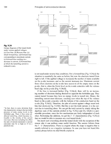
Fig. 9.24
Energy diagrams of the tunnel diode
under various applied voltages.
(a) Zero bias. (b) Reverse bias. (c)
Small forward bias. (d) Forward bias
corresponding to maximum current.
(e) Forward bias resulting in a
decrease in current. (f) Forward bias
at which the tunnelling current is
reduced to zero.
is not used under reverse bias conditions. For a forward bias [Fig. 9.24(c)] the
situation is essentially the same as before, but now the electrons tunnel from
right to left. If the applied voltage is increased, the number of states available
on the p-side increases, and so the current increases too. Maximum current
flows when electrons on the n-side have access to all the empty states on the
p-side, that is, when the Fermi level on the n-side coincides with the valence
band edge on the p-side [Fig. 9.24(d)].
If the bias is increased further [Fig. 9.24(e)], there will be an increas-
ing number of electrons finding themselves opposite the forbidden gap. They
cannot tunnel because they have no energy levels to tunnel into. Hence, the
tunnelling current must decrease, reaching zero when the top of the valence
band on the p-side coincides with the bottom of the conduction band on the
n-side [Fig. 9.24(f)]. Therefore, the plot of current against voltage must look
like that shown in Fig. 9.25(b). But this is not the total current; it is the cur-
∗
In fact, there is some deviation from rent due to tunnelling alone. We can get the total current by simply taking the
this characteristic owing to the inevitable algebraic sum of the currents plotted in Fig. 9.25(a) and (b), which is a per-
presence of some energy levels in the
forbidden gap. There is thus some ad- missible procedure, since the two mechanisms are fairly independent of each
ditional tunnelling, which becomes no- other. Performing the addition, we get the I – U characteristics [Fig. 9.25(c)]
ticeable in the vicinity of the current that we would be able to measure on a real tunnel diode. ∗
minimum. But even including this effect You know now everything about the tunnel diode with the exception of the
the ratio of current maximum to current
minimum may be as high as 15 in a reason why it can perform some useful function. The answer follows from
practical case. the I – U characteristics. There is a region where the slope is negative that is
usually referred to as a negative resistance. In case you have not heard this
curious phrase before we shall briefly explain it.