
Page 205 - Electrical Properties of Materials
P. 205
The Zener diode and the avalanche diode 187
be controlled by the impurity levels, this effect has applications whenever a
sudden increase in current is required at a certain voltage. The diode can there-
∗ There were, of course, no p–n junc-
fore be used as a voltage stabilizer or a switch. In the latter application it has
tions at the time. The mechanism was
the further advantage that the breakdown is not only sharp but occurs very suggested for bulk breakdown to which,
fast as well. The breakdown may occur by two distinct mechanisms: Zener incidentally, it does not apply. The ex-
breakdown or avalanche breakdown. planation turned out to be applicable to
breakdown in p–n junctions.
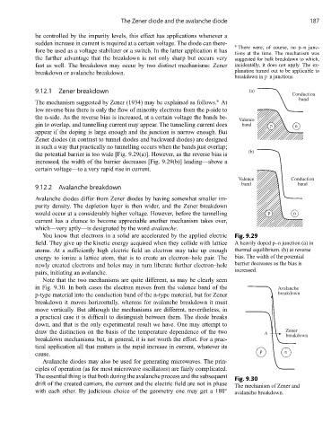
9.12.1 Zener breakdown (a)
Conduction
band
∗
The mechanism suggested by Zener (1934) may be explained as follows. At
low reverse bias there is only the flow of minority electrons from the p-side to
the n-side. As the reverse bias is increased, at a certain voltage the bands be- Valence
gin to overlap, and tunnelling current may appear. The tunnelling current does band p n
appear if the doping is large enough and the junction is narrow enough. But
Zener diodes (in contrast to tunnel diodes and backward diodes) are designed
in such a way that practically no tunnelling occurs when the bands just overlap;
(b)
the potential barrier is too wide [Fig. 9.29(a)]. However, as the reverse bias is
increased, the width of the barrier decreases [Fig. 9.29(b)] leading—above a
certain voltage—to a very rapid rise in current.
Valence Conduction
band band
9.12.2 Avalanche breakdown
Avalanche diodes differ from Zener diodes by having somewhat smaller im-
purity density. The depletion layer is then wider, and the Zener breakdown
would occur at a considerably higher voltage. However, before the tunnelling p n
current has a chance to become appreciable another mechanism takes over,
which—very aptly—is designated by the word avalanche.
You know that electrons in a solid are accelerated by the applied electric Fig. 9.29
field. They give up the kinetic energy acquired when they collide with lattice A heavily doped p–n junction (a) in
atoms. At a sufficiently high electric field an electron may take up enough thermal equilibrium. (b) at reverse
energy to ionize a lattice atom, that is to create an electron–hole pair. The bias. The width of the potential
newly created electrons and holes may in turn liberate further electron–hole barrier decreases as the bias is
increased.
pairs, initiating an avalanche.
Note that the two mechanisms are quite different, as may be clearly seen
in Fig. 9.30. In both cases the electron moves from the valence band of the Avalanche
p-type material into the conduction band of the n-type material, but for Zener breakdown
breakdown it moves horizontally, whereas for avalanche breakdown it must
move vertically. But although the mechanisms are different, nevertheless, in
a practical case it is difficult to distinguish between them. The diode breaks
down, and that is the only experimental result we have. One may attempt to
draw the distinction on the basis of the temperature dependence of the two A Zener
breakdown
breakdown mechanisms but, in general, it is not worth the effort. For a prac-
tical application all that matters is the rapid increase in current, whatever its
p n
cause.
Avalanche diodes may also be used for generating microwaves. The prin-
ciples of operation (as for most microwave oscillators) are fairly complicated.
The essential thing is that both during the avalanche process and the subsequent
Fig. 9.30
drift of the created carriers, the current and the electric field are not in phase The mechanism of Zener and
with each other. By judicious choice of the geometry one may get a 180 ◦ avalanche breakdown.