
Page 209 - Electrical Properties of Materials
P. 209
Field-effect transistors 191
is strongly reminiscent of that of anode current against grid voltage in a good
triode, the product of a bygone age when the subject of electronics was nice
and simple.
The physical picture yielding the I D versus U DS characteristics is a little
more complicated. As U DS increases at constant gate voltage, there are two
effects occurring simultaneously: (i) the drain current increases because U DS
has increased, a simple consequence of Ohm’s law; (ii) the drain current de-
creases because increased drain voltage means increased reverse bias and thus
a smaller channel for the current to flow. Now will the current increase or de-
crease? You might be able to convince yourself that when the channel is wide,
and the increase in U DS means only a relatively small decrease in the width
of the channel, the second effect is small, and the current increases. However,
as the channel becomes narrower the second effect gradually gains import-
ance, and the increase of I D with U DS slows down, as shown in Fig. 9.33(b).
At the so-called pinch-off voltage, the two effects cancel each other, and they
keep their balance for voltages beyond that. The current stays constant; it has
reached saturation. The actual value of the saturation current would naturally
depend on the gate voltage. At lower gate voltages the saturation current is
smaller.
The physical mechanism of current flow in an FET is entirely different from
that in a vacuum tube, but the characteristics are similar, and so is the equi-
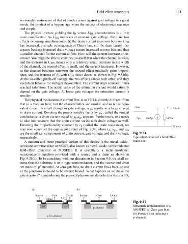
valent circuit. A small change in gate voltage, u gs , results in a large change Gate Drain
in drain current. Denoting the proportionality factor by g m , called the mutual
conductance, a drain current equal to g m u gs appears. Furthermore, one needs u gs g m u gs r d u ds
to take into account that the drain current varies with drain voltage as well.
Denoting the proportionality constant by r d (called the drain resistance), we
Source
may now construct the equivalent circuit of Fig. 9.34, where i d , u gs , and u ds
are the small a.c. components of drain current, gate voltage, and drain voltage, Fig. 9.34
respectively. Equivalent circuit of a field-effect
A modern and more practical variant of this device is the metal–oxide– transistor.
semiconductor transistor or MOST, also known as metal–oxide–semiconductor
field-effect transistor or MOSFET. It is essentially a metal–insulator–
semiconductor junction provided with a source and a drain as shown in
Fig. 9.35(a). To be consistent with our discussion in Section 9.9, we shall as-
sume that the substrate is an n-type semiconductor, and the source and drain
+
are made of p material. At zero gate bias, no drain current flows because one
of the junctions is bound to be reverse biased. What happens as we make the
gate negative? Remembering the physical phenomena described in Section 9.9,
(a) (b)
Source Gate Drain Source Gate Drain
Metal SiO 2
Fig. 9.35
p + p + Schematic representation of a
p-channel
MOSFET. (a) Zero gate bias.
(b) Forward bias inducing a
n-Si substrate
p-channel.