
Page 211 - Electrical Properties of Materials
P. 211
Field-effect transistors 193
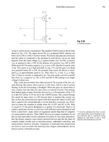
+U
0
S
M1
D
U U
in D out
M2
Fig. 9.38
S
ACMOSinverter.
owing to its low power consumption. The simplest CMOS circuit is the inverter
shown in Fig. 9.38. The upper device M1 is a p-channel MOS, whereas the
lower device M2 is of the n-channel variety. The drains and gates are connected,
and the source is connected to the substrate in each device. Let us see what
happens when the input voltage U in is approximately zero. For M2, a positive
U GS is required to turn it ON. In the absence of a positive U GS ,M2isOFF.
What about M1? It needs a negative U GS to turn it ON. But that is exactly what
it has. The source is at a high potential U 0 (say 5 V) and the gate is at about
zero potential hence M1 is ON, the potential drop across the device is small,
and U out is approximately equal to U 0 . Thus when U in is low, U out is high.
This is what an inverter is supposed to do. You may easily convince yourself
that when U in is equal to U 0 , M1 is OFF and M2 is ON leading to an output
voltage of about zero.
Why is this inverter better than other inverters? On account of the low cur-
rents flowing. But surely when a device is ON, there will be a lot of current
flowing. Is not the best analogy a floodgate? When the gates are closed there is
only a trickle, but when they are open, there is a torrent of water. This analogy
does indeed apply to many electronic devices (e.g. to the transistor of Fig. 9.15
or to the FET of Fig. 9.35) but not to the CMOS inverter. The current through
M1 cannot be large when it is ON because there is nowhere the current can
flow. In fact, the current must be equal to that flowing in M2 when it is OFF, and
that is equal to the current through a reverse biased p–n junction, say 50 nA.
And of course the situation is similar when M1 is OFF and M2 is ON. With
U 0 equal to 5 V, the power dissipation is a quarter of a microwatt. There is of
course a small gate current, as well, but it will still leave power dissipation well
∗
below a microwatt , many orders of magnitude smaller than that of competit- ∗ It must be admitted that there is some
ive semiconductor devices. Thus CMOS devices are natural candidates for all more appreciable power dissipation dur-
ing switching due to capacitors being
devices that must either involve extremely low power or very many transistors.
charged up, and there is also a brief
Into the former category come battery-powered devices and into the latter all interval when both devices are ON.
complex digital circuits such as microprocessors, embedded controllers, and
semiconductor memory elements. Computers in particular have transformed
our lives to such an extent that learning some elegant semiconductor device
physics seems a small price to pay.