
Page 215 - Electrical Properties of Materials
P. 215
Heterostructures 197
The energy diagram of Fig. 9.41(c) looks quite different from anything we
have seen so far. Not surprisingly, this junction has quite striking properties as
may be seen in Fig. 9.41(d), where the central part of the diagram is magnified.
The remarkable thing is that c B , the deepest point in the potential well, is
below the Fermi energy. Thus according to the rules of the game, the electron
density there is much higher than in any other parts of the two materials. The
second striking property is that the well is very narrow. How narrow? For the
materials usually used, the width of the well comes out of the calculations (they
are pretty complicated, one needs to solve simultaneously Poisson’s equation
in combination with Schrödinger’s equation) as about 8 nm, comparable with
atomic dimensions. So the electron is confined in one dimension. We have, in
∗
fact, a two-dimensional electron gas, which has discrete energy levels. In the ∗ The discrete character of the energy
present example we are showing just one such level. levels does not much affect the argu-
Let us return now to our original aim. We wanted to produce a field-effect ment here. They are, however, of great
importance for the Resonant Tunnelling
transistor which works faster than those using homojunctions on account of Diode to be discussed in Section 9.27
the higher mobility. So what kind of materials are we going to use? For the and for the latest versions of semicon-
undoped material we shall choose one which has a high mobility. GaAs with a ductor lasers which will come up in
2
–1 –1
bandgap of 1.43 eV and a mobility of 0.85 m V s at room temperature (up Section 12.7.
2
–1 –1
to about 7.5 m V s at 77 K) is clearly suitable for the purpose. The doped
material should have a considerably higher bandgap and must be suitable for
†
growing on GaAs. All these requirements are satisfied by Al x Ga 1–x As. With † Remember our discussion in Sec-
x = 0.3, the bandgap is 1.85 eV, E c is 0.28 eV, and E v is 0.15 eV. The dopant tion 8.6: Al is higher than both Ga and
is silicon. As in the periodic table, hence adding
Al to GaAs leads to a material of higher
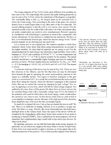
A schematic drawing of the device may be seen in Fig. 9.42. There are very
energy gap.
few electrons in the AlGaAs, and the few that there are may be eliminated
from beneath the gate by operating the metal–semiconductor junction in this
region as a Schottky barrier. This region is therefore analogous to the gate
oxide in a conventional FET. As a result, the current between the source and the
drain flows along the channel, where the electrons congregate in the undoped
GaAs. But can we control the current by changing the gate voltage? Yes, we source gate drain
can, by applying a reverse bias, which will lift the whole energy diagram. Not
doped Al GaAs
uniformly of course, there will be greater lift where there are fewer carriers, but
the essential thing is that with a reasonable voltage (say, 0.5 V), the bottom of channel
the potential well could be lifted above the Fermi energy, which would reduce undoped GaAs
the current to very close to zero. So this device could work as a fast switch or
as an amplifier in analogue circuits. Because of the high speed of the electrons, Fig. 9.42
these amplifiers may work up to the mm wavelength region.
A schematic drawing of a HEMT.
So much for n-channel devices. Can we have p-channel devices as well? We
can. There is no difficulty in doping AlGaAs so as to produce a p-type ma-
terial. But there is a snag. AlGaAs, like most semiconductors, has both heavy
and light holes in the valence band. Since the speed of the device will be de-
termined by the sluggishness of the heavy holes, there seems to be no point in
producing p-channel HEMTs. This is indeed true for most purposes, but let us
remember that complementary logic needs both n-type and p-type devices. So
what can be done?
By applying a pressure, we can shift the band edge in the energy diagram. In
particular, we can effectively suppress the heavy holes in favour of light holes.
In fact, there is no need actually to apply a pressure, as it may appear due to the
inherent properties of the junction. This is what actually happens when InGaAs