
Page 216 - Electrical Properties of Materials
P. 216
198 Principles of semiconductor devices
is grown on GaAs. Since the two materials have different lattice constants, a
strain will appear in the InGaAs layer, which will suppress the hole states at the
top of the valence band. By good luck the bandgap of InGaAs happens to be
smaller than that of GaAs. Hence a fast p-channel HEMT may be constructed
by doping an epitaxially grown GaAs layer with acceptors and then growing
a layer of undoped InGaAs on top. The p-channel will be made up of lighter
holes just inside the InGaAs layer.
What can we say about the future? As the new methods of production (MBE
and MOCVD) will be more widely used, heterojunctions will hardly cost more
than homojunctions. The point is that for economic reasons one wishes to avoid
multiple growth (remove the wafer, do some intermediate processing, and then
resume the growth) but it does not matter how complicated an individual run
is. So heterojunctions are here to stay.
9.16 Charge-coupled devices
Charge-coupled devices, abbreviated as CCDs, look very similar to MOS-
FETs, and in today’s world looking similar is half the battle. Since companies
are rather reluctant to invest in new types of manufacturing processes, a new
device that can be made by a known process and is compatible with existing
devices is an attractive proposition. CCDs were invented in 1969 at AT & T
Bell Laboratories, by Willard Boyle and George E. Smith (Nobel Prize, 2009).
At the time, they were working on something entirely different, semiconductor
U U U (a) bubble memories. However, an analogy between bubbles of charge and mag-
1 2 3
1 2 3 netic bubbles somehow suggested itself, and their first paper crucially listed
SiO
2
imaging devices as a possible application, as well as memory. In the end the
CCD succeeded beyond all expectations (while the bubble memory is largely
confined to history).
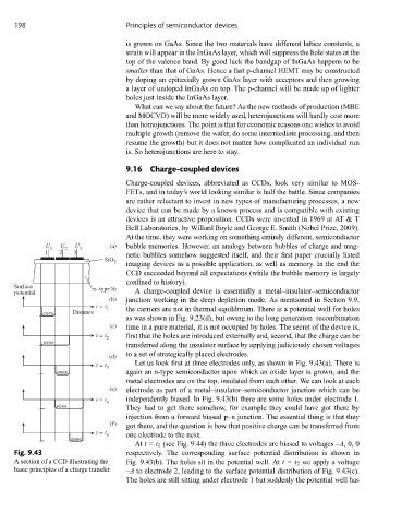
Surface n- type Si
potential A charge-coupled device is essentially a metal–insulator–semiconductor
(b) junction working in the deep depletion mode. As mentioned in Section 9.9,
t = t 1
Distance the carriers are not in thermal equilibrium. There is a potential well for holes
as was shown in Fig. 9.23(d), but owing to the long generation–recombination
(c) time in a pure material, it is not occupied by holes. The secret of the device is,
t = t first that the holes are introduced externally and, second, that the charge can be
2
transferred along the insulator surface by applying judiciously chosen voltages
to a set of strategically placed electrodes.
(d)
Let us look first at three electrodes only, as shown in Fig. 9.43(a). There is
t = t 3
again an n-type semiconductor upon which an oxide layer is grown, and the
metal electrodes are on the top, insulated from each other. We can look at each
(e) electrode as part of a metal–insulator–semiconductor junction which can be
t = t 4 independently biased. In Fig. 9.43(b) there are some holes under electrode 1.
They had to get there somehow, for example they could have got there by
injection from a forward biased p–n junction. The essential thing is that they
(f) got there, and the question is how that positive charge can be transferred from
t = t
5 one electrode to the next.
At t = t 1 (see Fig. 9.44) the three electrodes are biased to voltages –A,0,0
Fig. 9.43 respectively. The corresponding surface potential distribution is shown in
A section of a CCD illustrating the Fig. 9.43(b). The holes sit in the potential well. At t = t 2 we apply a voltage
basic principles of a charge transfer. –A to electrode 2, leading to the surface potential distribution of Fig. 9.43(c).
The holes are still sitting under electrode 1 but suddenly the potential well has