
Page 219 - Electrical Properties of Materials
P. 219
The Gunn effect 201
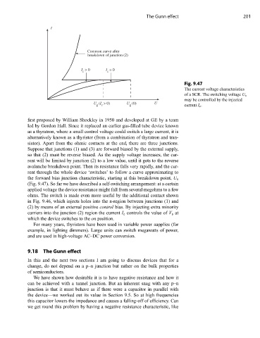
I
Common curve after
breakdown of junction (2)
I > 0 I = 0
c c
Fig. 9.47
The current voltage characteristics
of a SCR. The switching voltage U s
may be controlled by the injected
U (I > 0) U (0) U
g c g current I c .
first proposed by William Shockley in 1950 and developed at GE by a team
led by Gordon Hall. Since it replaced an earlier gas-filled tube device known
as a thyratron, where a small control voltage could switch a large current, it is
alternatively known as a thyristor (from a combination of thyratron and tran-
sistor). Apart from the ohmic contacts at the end, there are three junctions.
Suppose that junctions (1) and (3) are forward biased by the external supply,
so that (2) must be reverse biased. As the supply voltage increases, the cur-
rent will be limited by junction (2) to a low value, until it gets to the reverse
avalanche breakdown point. Then its resistance falls very rapidly, and the cur-
rent through the whole device ‘switches’ to follow a curve approximating to
the forward bias junction characteristic, starting at this breakdown point, U s
(Fig. 9.47). So far we have described a self-switching arrangement: at a certain
applied voltage the device resistance might fall from several megohms to a few
ohms. The switch is made even more useful by the additional contact shown
in Fig. 9.46, which injects holes into the n-region between junctions (1) and
(2) by means of an external positive control bias. By injecting extra minority
carriers into the junction (2) region the current I c controls the value of V s at
which the device switches to the on position.
For many years, thyristors have been used in variable power supplies (for
example, in lighting dimmers). Large units can switch megawatts of power,
and are used in high-voltage AC–DC power conversion.
9.18 The Gunn effect
In this and the next two sections I am going to discuss devices that for a
change, do not depend on a p–n junction but rather on the bulk properties
of semiconductors.
We have shown how desirable it is to have negative resistance and how it
can be achieved with a tunnel junction. But an inherent snag with any p–n
junction is that it must behave as if there were a capacitor in parallel with
the device—we worked out its value in Section 9.5. So at high frequencies
this capacitor lowers the impedance and causes a falling-off of efficiency. Can
we get round this problem by having a negative resistance characteristic, like