
Page 214 - Electrical Properties of Materials
P. 214
196 Principles of semiconductor devices
) a ( A B ) b (
E ΔE E F
FA c
E
FB
ΔE
v
(c) (d)
c
A
Δ E c E
c F c A
B
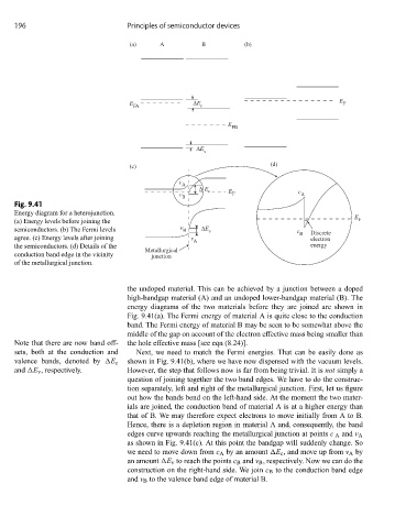
Fig. 9.41
Energy diagram for a heterojunction. E
(a) Energy levels before joining the F
semiconductors. (b) The Fermi levels v B ΔE v c Discrete
agree. (c) Energy levels after joining v B electron
A
the semiconductors. (d) Details of the energy
Metallurgical
conduction band edge in the vicinity junction
of the metallurgical junction.
the undoped material. This can be achieved by a junction between a doped
high-bandgap material (A) and an undoped lower-bandgap material (B). The
energy diagrams of the two materials before they are joined are shown in
Fig. 9.41(a). The Fermi energy of material A is quite close to the conduction
band. The Fermi energy of material B may be seen to be somewhat above the
middle of the gap on account of the electron effective mass being smaller than
Note that there are now band off- the hole effective mass [see eqn (8.24)].
sets, both at the conduction and Next, we need to match the Fermi energies. That can be easily done as
valence bands, denoted by E c shown in Fig. 9.41(b), where we have now dispensed with the vacuum levels.
and E v , respectively. However, the step that follows now is far from being trivial. It is not simply a
question of joining together the two band edges. We have to do the construc-
tion separately, left and right of the metallurgical junction. First, let us figure
out how the bands bend on the left-hand side. At the moment the two mater-
ials are joined, the conduction band of material A is at a higher energy than
that of B. We may therefore expect electrons to move initially from A to B.
Hence, there is a depletion region in material A and, consequently, the band
edges curve upwards reaching the metallurgical junction at points c A and v A
as shown in Fig. 9.41(c). At this point the bandgap will suddenly change. So
we need to move down from c A by an amount E c , and move up from v A by
an amount E v to reach the points c B and v B , respectively. Now we can do the
construction on the right-hand side. We join c B to the conduction band edge
and v B to the valence band edge of material B.