
Page 210 - Electrical Properties of Materials
P. 210
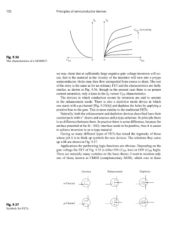
192                           Principles of semiconductor devices

                                                        I       I
                                                         D      D

                                                                                 U  decreasing
                                                                                  GS


     Fig. 9.36
                                        U               0      0                    U
     The characteristics of a MOSFET.     GS                                         DS


                                   we may claim that at sufficiently large negative gate voltage inversion will oc-
                                   cur, that is the material in the vicinity of the insulator will turn into a p-type
                                   semiconductor. Holes may then flow unimpeded from source to drain. The rest
                                   of the story is the same as for an ordinary FET and the characteristics are fairly
                                   similar, as shown in Fig. 9.36, though in the present case there is no proper
                                   current saturation, only a knee in the I D versus U DS characteristics.
                                     The devices in which conduction occurs by inversion are said to operate
                                   in the enhancement mode. There is also a depletion mode device in which
                                   one starts with a p-channel [Fig. 9.35(b)] and depletes the holes by applying a
                                   positive bias to the gate. This is more similar to the traditional FETs.
                                     Naturally, both the enhancement and depletion devices described have their
                                                  +
                                   counterparts with n drains and sources and p-type substrate. In principle there
                                   is no difference between them. In practice there is some difference, because the
                                   surface potential at the Si - SiO 2 interface tends to be positive, thus it is easier
                                   to achieve inversion in an n-type material.
                                     Having so many different types of FETs has tested the ingenuity of those
                                   whose job it is to think up symbols for new devices. The solutions they came
                                   up with are shown in Fig. 9.37.
                                     Applications for performing logic functions are obvious. Depending on the
                                   gate voltage the FET of Fig. 9.35 is either ON (U DS low) or OFF (U DS high).
                                   There are naturally many varieties on the basic theme; I want to mention only
                                   one of them, known as CMOS (complementary MOS), which rose to fame


                                                  Junction       Enhancement        Depletion


                                       n-Channel


                                       p-Channel
     Fig. 9.37
     Symbols for FETs.