
Page 208 - Electrical Properties of Materials
P. 208
190 Principles of semiconductor devices
+ –
Depletion
regions
Signal Gate n-type
input ~ semiconductor
Drain
Source
I DS
+
n - contact
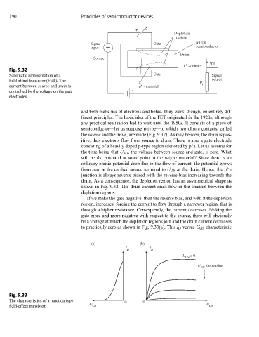
Fig. 9.32
Schematic representation of a Gate Signal
field-effect transistor (FET). The output
R
current between source and drain is p - material L
+
controlled by the voltage on the gate – +
electrodes.
and both make use of electrons and holes. They work, though, on entirely dif-
ferent principles. The basic idea of the FET originated in the 1920s, although
any practical realization had to wait until the 1950s. It consists of a piece of
semiconductor—let us suppose n-type—to which two ohmic contacts, called
the source and the drain, are made (Fig. 9.32). As may be seen, the drain is pos-
itive: thus electrons flow from source to drain. There is also a gate electrode
+
consisting of a heavily doped p-type region (denoted by p ). Let us assume for
the time being that U SG , the voltage between source and gate, is zero. What
will be the potential at some point in the n-type material? Since there is an
ordinary ohmic potential drop due to the flow of current, the potential grows
+
from zero at the earthed source terminal to U DS at the drain. Hence, the p n
junction is always reverse biased with the reverse bias increasing towards the
drain. As a consequence, the depletion region has an asymmetrical shape as
shown in Fig. 9.32. The drain current must flow in the channel between the
depletion regions.
If we make the gate negative, then the reverse bias, and with it the depletion
region, increases, forcing the current to flow through a narrower region, that is
through a higher resistance. Consequently, the current decreases. Making the
gate more and more negative with respect to the source, there will obviously
be a voltage at which the depletion regions join and the drain current decreases
to practically zero as shown in Fig. 9.33(a). This I D versus U GS characteristic
(a) (b)
I I
D D
U = 0
GS
U decreasing
GS
Fig. 9.33
The characteristics of a junction type 0 0
U U
field-effect transistor. GS DS