
Page 212 - Electrical Properties of Materials
P. 212
194 Principles of semiconductor devices
9.15 Heterostructures
All the devices mentioned so far have been made using the same material.
Some properties of the material were tampered with, for example doping made
one part of the material n-type and another part p-type, but the energy gap
always remained the same. We may call such structures homostructures in con-
trast with heterostructures, which consist of materials of different energy gaps.
Is it in any way desirable to change the energy gap? The simple answer is, yes,
it gives us a new degree of freedom.
In order to appreciate the difference between these two types of junc-
tions, let us first redo the construction that leads to the built-in voltage in
homojunctions and then repeat the exercise for heterojunctions.
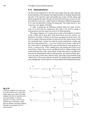
The energy diagrams of a p-type and an n-type semiconductor are shown
in Fig. 9.39(a) next to each other. Their Fermi levels are at E Fp and E Fn ,re-
spectively. Next [Fig. 9.39(b)], we join them and equate the Fermi levels. The
built-in voltage is the same whether we look at it from the valence band or from
the conduction band. Assume now that the p-type material has a higher gap
than the n-type material (E gp > E gn ) but its Fermi level relative to the top of
the valence band is unchanged. The n-type material has the same properties as
before, as shown in Fig. 9.39(c). Joining them and equating their Fermi levels
leads to Fig. 9.39(d). It may now be seen that the built-in voltage is higher in the
conduction band than in the valence band. For the holes, there is no difference
between the homojunction and the heterojunction: the amount of hole injec-
tion is the same in both cases. But the energy gap of the p-type material being
wider in Fig. 9.39(c) means that the electrons see a higher barrier against them
and, consequently, electron injection is much smaller in the heterojunction than
) a ( ) b (
E g E g E g
E Fn
E Fn – E Fp
E Fp E Fp
0 0 0
E – E Fp
Fn
) c ( ) d (
Fig. 9.39
(a) Energy diagrams of a p-type and E gp E gp
an n-type material next to each other; E gn
E
energy gaps are the same. (b) Energy Fn E – E Fp
Fn
gp
diagram when the two materials in (a) + E – E gn
are joined together. (c) Energy
diagrams of a p-type and an n-type E Fp E fp
material next to each other; energy 0 0 0
gaps are different. (d) Energy diagram E – E
when the two materials in (c) are Fn Fp
joined together.