
Page 213 - Electrical Properties of Materials
P. 213
Heterostructures 195
in the homojunction. Is this good? If we imagine that this is the emitter–base
junction of a p–n–p transistor then this is certainly something desirable. The
hole current from emitter to base is the current upon which the operation of
the transistor is based. We need that. The electron current from base to emitter,
however, does no good. We are better off without it. The conclusion is that by
using a heterojunction we can produce a transistor with properties superior to
that of a homojunction. The transistor thus obtained has even got a name. It is
known as HBT or Heterostructure Bipolar Transistor.
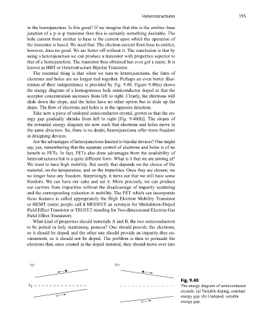
The essential thing is that when we turn to heterojunctions, the fates of
electrons and holes are no longer tied together. Perhaps an even better illus-
tration of their independence is provided by Fig. 9.40. Figure 9.40(a) shows
the energy diagram of a homogeneous bulk semiconductor doped so that the
acceptor concentration increases from left to right. Clearly, the electrons will
slide down the slope, and the holes have no other option but to slide up the
slope. The flow of electrons and holes is in the opposite direction.
Take now a piece of undoped semiconductor crystal, grown so that the en-
ergy gap gradually shrinks from left to right [Fig. 9.40(b)]. The slopes of
the potential energy diagram are now such that electrons and holes move in
the same direction. So, there is no doubt, heterojunctions offer more freedom
in designing devices.
Are the advantages of heterojunctions limited to bipolar devices? One might
say, yes, remembering that the separate control of electrons and holes is of no
benefit to FETs. In fact, FETs also draw advantages from the availability of
heterostructures but in a quite different form. What is it that we are aiming at?
We want to have high mobility. But surely that depends on the choice of the
material, on the temperature, and on the impurities. Once they are chosen, we
no longer have any freedom. Surprisingly, it turns out that we still have some
freedom. We can have our cake and eat it. More precisely, we can produce
our carriers from impurities without the disadvantage of impurity scattering
and the corresponding reduction in mobility. The FET which can incorporate
these features is called appropriately the High Electron Mobility Transistor
or HEMT (some people call it MODFET an acronym for Modulation-Doped
Field Effect Transistor or TEGFET standing for Two-dimensional Electron Gas
Field Effect Transistor).
What kind of properties should materials A and B, the two semiconductors
to be joined in holy matrimony, possess? One should provide the electrons,
so it should be doped, and the other one should provide an impurity-free en-
vironment, so it should not be doped. The problem is then to persuade the
electrons that, once created in the doped material, they should move over into
(a) (b)
Fig. 9.40
E The energy diagram of semiconductor
F
crystals. (a) Variable doping, constant
energy gap. (b) Undoped, variable
energy gap.