
Page 218 - Electrical Properties of Materials
P. 218
200 Principles of semiconductor devices
new charge packet entering the first electrode. With 3000 electrodes in a line,
we can have 1000 charge packets stored in the device.
How many elements can be in series? It depends on the amount of charge
lost at each transfer. And that is actually the limiting factor in speed as well.
If we try to transfer the charge too quickly, some of it will get stuck and the
information will be gradually corrupted. The troublemakers are the surface
states again. They trap and release charge carriers randomly, thereby interfering
with the stored information. Thus, the best thing is to keep the charge away
from the surface. This can be done by inserting an additional p-channel into
the junction in much the same way as in Fig. 9.35(b). The potential minimum is
then in the p-channel, which under reverse bias conditions is entirely depleted
of its ‘own’ carriers and is ready to accept charge packets from the outside.
These are called buried-channel devices.
What about other limitations? Well, there is a maximum amount of charge
storable above which the potential minimum disappears. There is a minimum
frequency, with which the charge can be transferred, below which the informa-
tion is corrupted by the thermally generated carriers. There is also a minimum
size for each cell determined by tunnelling effects (if the cells are too close to
each other) and dielectric breakdown (if the insulator is too thin).
What can CCDs be used for? The most important application is for optical
imaging for which we do of course need a two-dimensional array. If a picture
is focused upon the surface of the device (which in this case has transparent
electrodes) the incident light creates electron–hole pairs proportional to its in-
tensity. The process now has two steps: the ‘integrate’ period, during which U 1
is set to a negative voltage and the holes (in practical devices electron packets
are used and everything is the other way round but the principles are the same)
are collected in the potential minima, and the ‘readout’ period, during which
the information, is read out. Light may still be incident upon the device during
readout, but if the readout period is much shorter than the integration period,
the resulting distortions of the video signal are negligible.
It may be worth mentioning
How many elements can we have? CCD sizes have grown rapidly. Arrays
here that CCDs can also be used
containing 16 MP (i.e. 4000 pixels x 4000 pixels) are common nowadays,
as detectors for high energy
and there is no reason to suppose there will not be further increases. The de-
particles, which might simultan-
velopment of the CCD and its incorporation into low-cost personal cameras
eously knock out thousands of has transformed our view of photography. Once an expensive luxury that re-
electron-hole pairs.
quired a professional armed with expensive equipment, the classical portrait
photograph is a thing of the past. Anyone can take a high quality photograph
(1) (2) (3)
or video, and more importantly replicate it, enhance it electronically, incor-
p n p n porate it into documents and presentations, and share it with others. These
developments have sounded the death-knell for the film industry, and the cam-
Injecting
contact era industry itself is under attack as mobile phones increasingly combine the
I
c simple operation of acquiring the image with the more sophisticated function
of communicating it. Surprisingly, photographers have survived, since there is
still one day—the wedding day—where only the professional will do.
+ –
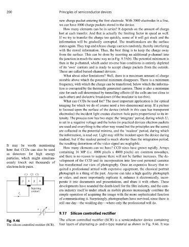
9.17 Silicon controlled rectifier
Fig. 9.46 The silicon controlled rectifier (SCR) is a semiconductor device containing
The silicon controlled rectifier (SCR). four layers of alternating p- and n-type material as shown in Fig. 9.46. It was