
Page 220 - Electrical Properties of Materials
P. 220
202 Principles of semiconductor devices
that of a tunnel diode, in a bulk semiconductor? This is a long-established El
Dorado of semiconductor device engineers. Nearly all semiconductors should
behave like this.
Look again at an E–k curve that we drew earlier [Fig. 7.12(a)]. If this rep-
resents the conduction band, the electrons will be clustered about the lowest
energy state: E =0, k = 0. Now apply a field in the x-direction which accel-
erates the electrons, so their momentum (which, as we have mentioned before,
is proportional to k) will increase as well. This means that our electrons are
climbing up the E–k curve. At a certain point the effective mass changes sign
as shown in Fig. 7.12(c). Now the effective mass is just a concept we intro-
duce to say how electrons are accelerated by a field; so this change of sign
means that the electrons go the other way. Current opposing voltage is a neg-
ative resistance situation. It seems that there should be a good chance of any
semiconductor behaving like this, but in fact so far this effect has not been
discovered. The reason must be that the electrons move for only a short time
without collisions. So to get within this time into the negative mass region,
very high fields are necessary, which causes some other trouble, for example
breakdown or thermal disintegration.
As a matter of fact, we do not really need to send our electron into the negat-
ive mass region to have a negative differential resistance. If the effective mass
of the electron increases fast enough as a function of the electric field, then
the reduced mobility (and conductivity) may lead to a reduction of current—
and that is a negative differential resistance, so there seems no reason why our
∗
device could not work in the region where m tends rapidly towards infinity. It
is a possibility, but experiments have so far stubbornly refused to display the
effect.
An improvement on the latter idea was put forward by Watkins, Ridley, and
Hilsum, who suggested that electrons excited into a subsidiary valley of GaAs
(see Fig. 8.10) might do the trick. The curvature at the bottom of this valley is
smaller; so the electrons acquire the higher effective mass that is our professed
aim. In addition there is a higher density of states (it is proportional to m ∗3/2 );
and furthermore, it looks quite plausible that, once an electron is excited into
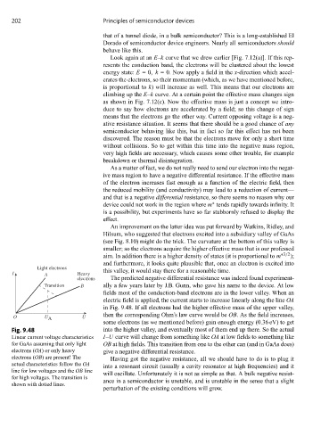
Light electrons
I A Heavy this valley, it would stay there for a reasonable time.
electrons The predicted negative differential resistance was indeed found experiment-
Transition B ally a few years later by J.B. Gunn, who gave his name to the device. At low
fields most of the conduction-band electrons are in the lower valley. When an
electric field is applied, the current starts to increase linearly along the line OA
in Fig. 9.48. If all electrons had the higher effective mass of the upper valley,
then the corresponding Ohm’s law curve would be OB. As the field increases,
O U A U
some electrons (as we mentioned before) gain enough energy (0.36 eV) to get
Fig. 9.48 into the higher valley, and eventually most of them end up there. So the actual
Linear current voltage characteristics I–U curve will change from something like OA at low fields to something like
for GaAs assuming that only light OB at high fields. This transition from one to the other can (and in GaAs does)
electrons (OA) or only heavy give a negative differential resistance.
electrons (OB) are present! The Having got the negative resistance, all we should have to do is to plug it
actual characteristics follow the OA
into a resonant circuit (usually a cavity resonator at high frequencies) and it
line for low voltages and the OB line
will oscillate. Unfortunately it is not as simple as that. A bulk negative resist-
for high voltages. The transition is
ance in a semiconductor is unstable, and is unstable in the sense that a slight
shown with dotted lines.
perturbation of the existing conditions will grow.