
Page 225 - Electrical Properties of Materials
P. 225
Microelectronic circuits 207
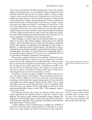
mask on top, and illuminate it by ultraviolet light [Fig. 9.53(b)]. The mask has
opaque and transparent areas, so it can define the region of photoresist upon
which the ultraviolet light can fall. It is usually a pattern of chrome on glass
or quartz, drawn using an electron beam writing system at a size that may be
significantly larger than the one finally required. The pattern is reduced using
a rather sophisticated ‘enlarger’ operating backwards. The dies are printed in a
step-and-repeat mode, so the patterning system is known as a ‘stepper’. Origin-
ally, mercury arc lamps (with a deep-UV wavelength of 365 nm at the ‘I’ line)
were used as light sources. ArF lasers are now common; since their emission
wavelength (193 nm) lies in the vacuum ultraviolet, evacuated light paths are
required. Immersion lenses (which have higher numerical aperture and hence
can form a smaller focused spot) are used to reduce the feature size still fur-
ther. Some of these techniques are discussed in more detail in Section 9.24. As
a result, equipment for lithography is now extremely expensive.
Other techniques are used to make sure the reduced feature size is main-
tained on the device itself. Plasma etching is used in place of wet chemical
etching to ensure that features do not broaden when the pattern is transferred
into the layer beneath. Ion implantation and annealing are used in place of
diffusion, to reduce the spread of buried features. Self-alignment is used to
eliminate the spaces that must normally be allowed between features on differ-
ent mask layers. Linewidths (0.5 μm in 1990) are now staggeringly small; 22
nm linewidth reached production in 2012 and 14 nm is predicted for 2014 by
the International Technology Roadmap for Semiconductors.
Photoresists are organic compounds whose solubility is affected by expos-
ure to ultraviolet light. We are using here a positive photoresist in which the
∗
exposed areas can be washed away by a suitable developer. After this opera- ∗ For a negative photoresist, as may be
tion, we are left with two windows in the photoresist, as shown in Fig. 9.53(c). expected, the unexposed areas are sol-
uble.
The one chemical that readily attacks SiO 2 is hydrofluoric acid (HF), but it
does not dissolve the photoresist. Hence, the windows in the resist can be
turned into windows in the SiO 2 by etching with HF [Fig. 9.53(d)] and the
remaining photoresist may then be removed [Fig. 9.53(e)].
The purpose of all these operations, starting with oxidation, was to get ac-
cess to the epitaxial layer at selected places. The next operation that makes use
of these windows is diffusion. The silicon is sealed into a clean furnace tube,
containing a volatile form of the required doping material. It is then heated for
a prescribed time, and the impurity diffuses into the surface. This is a solid
state diffusion process, and the important thing is that it is completely inhib-
ited in the oxide covered regions. For the p-type doping we want here we could
+
◦
use boron bromide (BBr 3 ) heated to about 1100 C. The emerging p region is
showninFig.9.53(f). Note that there is lateral diffusion
+
The oxide layer has now done its duty, so it may be removed, and we are as well, so the p region extends
ready to perform the next operation, which is to provide a window for base somewhat under the oxide layer.
diffusion. The steps are again oxidation, photoresist coating, masking, illu- The aim of this diffusion is to
mination by ultraviolet light, removal of the exposed photoresist, and removal isolate the present transistor from
of the oxide layer underneath. Then comes the p-type diffusion with which the others made on the same chip.
stage shown in Fig. 9.53(g) is reached.
A further repetition of the technique leads to a window for a diffusion of
+
+
phosphorus, which forms the n emitter region [Fig. 9.53(h)]. The n –p–n tran-
sistor is now ready, though it still needs to be connected to other elements on