
Page 226 - Electrical Properties of Materials
P. 226
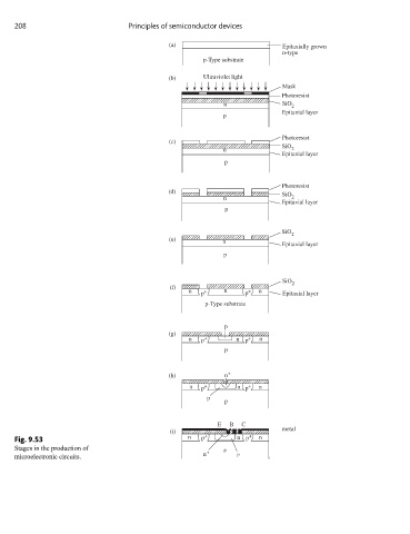
208                           Principles of semiconductor devices

                                             (a)                           Epitaxially grown
                                                                           n-type
                                                      p-Type substrate

                                             (b)      Ultraviolet light
                                                                           Mask
                                                                           Photoresist
                                                           n               SiO 2
                                                                           Epitaxial layer
                                                           p

                                                                           Photoresist
                                             (c)
                                                                           SiO
                                                           n                 2
                                                                           Epitaxial layer
                                                            p

                                                                           Photoresist
                                             (d)                           SiO
                                                           n                 2
                                                                           Epitaxial layer
                                                            p

                                                                           SiO 2
                                             (e)
                                                           n
                                                                           Epitaxial layer
                                                           p

                                                                           SiO 2
                                             (f)
                                                  n   p +   n    p +  n    Epitaxial layer
                                                       p-Type substrate


                                                            p
                                             (g)
                                                  n   p +      n  p +  n
                                                            p


                                             (h)            n +
                                                  n   p +      n  p +  n
                                                       p
                                                            p


                                                          E  B  C
                                             (i)                           metal
     Fig. 9.53                                    n   p +      n  p +  n
     Stages in the production of                       +    p
     microelectronic circuits.                        n        p