
Page 227 - Electrical Properties of Materials
P. 227
Microelectronic circuits 209
the same chip; so we need some electrodes. This may be done by forming three
more windows and evaporating a metal, usually aluminium, for the emitter,
base, and collector contacts. The finished transistor is shown in Fig. 9.53(i).
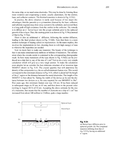
In practice, the above structure is rarely used because of two major dis-
advantages, first the parasitic p–n–p transistor (formed by the base, collector,
and substrate regions) may draw away current to the substrate, and second there
is a long path of high resistance from the emitter to the collector. The remedy
+
is to diffuse an n buried layer into the p-type substrate prior to the epitaxial
growth of the n-layer. Thus, the starting point is as shown in Fig. 9.54(a) instead
of that in Fig. 9.53(a).
+
There is also an additional n diffusion, following the emitter diffusion,
leading to the final product shown in Fig. 9.54(b). Note that there is a more
modern technique of doping called ion implantation. As the name implies, this
involves the implantation (in fact, shooting them in with high energy) of ions
to wherever the impurities are needed.
Now we know how to make one transistor. The beauty of the technique is
that it can make simultaneously millions or billions of transistors. The inform-
ation where the circuits reside is contained in the corresponding photographic
mask. So how many transistors of the type shown in Fig. 9.54(b) can be pro-
2
duced on a chip that is, say, of the size of 1 cm ? Let us do a very, very simple
calculation which will give us a very rough answer. To make the calculation
even simpler let us consider the less elaborate structure of an inversion type
MOSFET shown in Fig. 9.55. The crucial quantity that will determine the
density of the components is a, the so-called minimum feature size. This would
correspond to the minimum distance in Fig. 9.55, which is about half the length
+
of the p region or the distance between the metal electrodes. The length of the
MOSFET is then about 9a. Taking the width of the device as 4a and the dis-
2
tance between two devices as a, the area required for one MOSFET is 50a .
Five years ago, this minimum feature size was 120 nm. It has been reduced
in subsequent stages to 95 nm, to 65 nm, and then down to the present value
(writing in August 2013) of 32 nm. Accepting the above estimate for the size
2
of a transistor, that means that the number of elements on a chip of 1 cm has
increased from about 140 million to 2 billion, quite a large number.
(a) n Epitaxial layer
n +
Buried layer
p
(b) E B C
Fig. 9.54
n p + n + n p + n (a) Buried layer diffusion prior to
epitaxial growth. (b) The completed
transistor differing from that of
p
Fig. 9.53 by having an additional
+
n region.