
Page 232 - Electrical Properties of Materials
P. 232
214 Principles of semiconductor devices
FinFET
Source
Drain
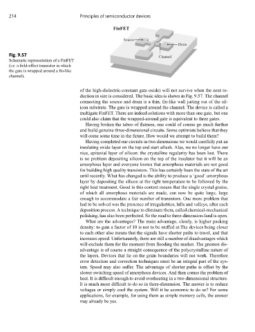
Fig. 9.57 Gate
Channel
Schematic representation of a FinFET
(i.e. a field-effect transistor in which
the gate is wrapped around a fin-like
channel).
of the high-dielectric-constant gate oxide) will not survive when the next re-
duction in size is considered. The basic idea is shown in Fig. 9.57. The channel
connecting the source and drain is a thin, fin-like wall jutting out of the sil-
icon substrate. The gate is wrapped around the channel. The device is called a
multigate FinFET. There are indeed solutions with more than one gate, but one
could also claim that the wrapped-around gate is equivalent to three gates.
Having broken the taboo of flatness, one could of course go much further
and build genuine three-dimensional circuits. Some optimists believe that they
will come some time in the future. How would we attempt to build them?
Having completed our circuits in two dimensions we would carefully put an
insulating oxide layer on the top and start afresh. Alas, we no longer have our
nice, epitaxial layer of silicon: the crystalline regularity has been lost. There
is no problem depositing silicon on the top of the insulator but it will be an
amorphous layer and everyone knows that amorphous materials are not good
for building high quality transistors. This has certainly been the state of the art
until recently. What has changed is the ability to produce a ‘good’ amorphous
layer by depositing the silicon at the right temperature to be followed by the
right heat treatment. Good in this context means that the single crystal grains,
of which all amorphous materials are made, can now be quite large, large
enough to accommodate a fair number of transistors. One more problem that
had to be solved was the presence of irregularities, hills and valleys, after each
deposition process. A technique to eliminate them, called chemical-mechanical
polishing, has also been perfected. So the road to three-dimension-land is open.
What are the advantages? The main advantage, clearly, is higher packing
density: to gain a factor of 10 is not to be sniffed at.The devices being closer
to each other also means that the signals have shorter paths to travel, and that
increases speed. Unfortunately, there are still a number of disadvantages which
will exclude them for the moment from flooding the market. The greatest dis-
advantage is of course a straight consequence of the polycrystalline nature of
the layers. Devices that lie on the grain boundaries will not work. Therefore
error detection and correction techniques must be an integral part of the sys-
tem. Speed may also suffer. The advantage of shorter paths is offset by the
slower switching speed of amorphous devices. And then comes the problem of
heat. It is difficult enough to avoid overheating in a two-dimensional structure.
It is much more difficult to do so in three-dimension. The answer is to reduce
voltages or simply cool the system. Will it be economic to do so? For some
applications, for example, for using them as simple memory cells, the answer
may already be yes.