
Page 237 - Electrical Properties of Materials
P. 237
Nanoelectronics 219
give you some indication of how it has been done. The technique is that of
Micro-Electro-Mechanical Systems, discussed earlier, but on a much smaller
scale so that we can replace the ‘Micro’ by ‘Nano’ arriving at the field of
∗
NEMS. The bottom-up approach is based on a small cantilever that can actu- ∗ The small cantilever may also serve as
ally capture an atom off the surface of some material and deposit it at another the basis of a new type of memory prom-
ising gigabytes of information on a few
place. The principles followed are that of the atomic force microscope.
square centimetres. Several companies,
There is no doubt that successful experiments have been done and a lot including IBM, made progress in that
has been learned but that is still a far cry from building useful devices in a direction. The information is written by a
reliable manner. Do we know the laws governing the nanometre scale? Yes, of sharp tip perched at the end of the canti-
lever dipping into a polymer and creating
course, they are the laws of quantum mechanics. We know the basic equations,
apit. Thepresenceofapitmay then be
but computers are just not powerful enough to get even near to solving them regarded as a one and the absence of a
for practical situations. So far in this course we have been able to manage pit as a zero. Reading is also done by
by injecting no more than a small amount of quantum mechanics. We needed a tip relying on a change of electrical
some basic tenets in order to explain the mechanism of conduction, the role resistance when it enters the pit.
of the periodic structure of atoms, the concept of tunnelling, etc. But having
accepted the notion of conduction and valence bands, the presence of two kinds
of carriers, energy gaps, impurity levels and so on, we could really use the
familiar classical picture. It does not really stretch our magination to the limits
to ‘see’ holes diffusing across the base region. We may legitimately boast to
have tamed quantum mechanics when dimensions are above about 50 nm. For
structures smaller than that the taming has just began. One hopes that it will
continue successfully.
I shall now discuss in a little more detail one of the devices that needs some
structure on the nanoscale. It bears some resemblance to the High-Electron-
Mobility-Transistor discussed in Section 9.15. The only essential difference,
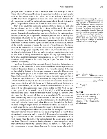
as shown in Fig. 9.60(a), is that the gate electrode is now split. There are now (a)
three finger-gates placed close to each other, where each finger-gate can be source split gate drain
biased independently. Let us have reverse bias on the outer gates, so there is n-type GaAlAs
undoped GaAs
a depletion layer below them. This means that the charge sheet sticking to the
semi-insulating
AlGaAs/GaAs boundary will have discontinuities. If there are no charges, there GaAs
is no current. So how will this device work? Let me quickly add that the inner (b)
gate is forward biased, so that the potential distribution between source and G1 G2 G3
drain will have the approximate shape shown in Fig. 9.60(b). Well, we have
a lower potential in the middle, but will that help? It will if the dimensions
are sufficiently small—then electrons may tunnel through the barriers. Does Fig. 9.60
this mean that the current will flow as in a tunnel diode? In one sense yes, (a) Schematic representation of a
Lateral Resonant Tunnelling
because tunnelling is necessary for the existence of electron flow. It is different,
Transistor; (b) Energy diagram
though, in another sense. In the tunnel diode the energy levels of the electrons
influenced by the voltages on the
were nigh infinitely close to each other. The current depended on the density
split electrodes.
of states. With gate fingers around 20–50 nm the electrons are confined to such
a small range that the individual energy levels can be distinguished.
One mode of operation is where the potentials at the outer gates and between
the source and the drain are fixed and the inner gate potential is varied, that is
the depth of the potential well is controlled. The energy levels are determined
by the confinement, so their positions are fixed relative to the bottom of the
well. Hence, when the depth of the well is changed, the energy levels move up
and down. There will be current flowing whenever a given energy level inside
the well matches that of the electrons outside the barrier. The name given to
this phenomenon is resonant tunnelling, and the device shown schematically