
Page 239 - Electrical Properties of Materials
P. 239
Nanoelectronics 221
two-dimensional sheet of graphite or can be regarded as a carbon nanotube un-
(a)
folded. It has a number of remarkable properties, which are being explored at
a number of research laboratories around the world. It has odd properties, for
example displaying the quantum Hall effect (to be discussed in Section 11.8.6)
E s E F
at room temperature. It is a semiconductor but there is no gap between the
valence and conduction bands. The density-of-state functions are two inverted
cones meeting at the line separating the two bands. The particles, electrons or
holes, resemble in some respects photons. They move with a constant velocity
which is independent of their kinetic energy. Even at room temperature they
scatter little, so that within a range, comparable with distances in a transistor, Insulators
they can be regarded as ballistic particles. Can one make ballistic transistors
out of graphene? Perhaps. One problem is to have a regime in which no current
flows. If there is no energy gap, the current cannot be stopped. This problem (b)
has been overcome by introducing constrictions in the material, which turn
out to be equivalent to gaps. It is too early to say what kind of devices might eVa = E s
emerge. They certainly belong to nanoelectronics since the device sizes might
be between 10 and 50 nm.
The third device is the Single Electron Transistor which, strictly speaking,
does not belong to this chapter since the materials involved are metals and
insulators not semiconductors. On the other hand they can only work when
the dimensions are in the nanometre region so it is not unreasonable to dis- Metal
cuss them here. The effect upon which these devices are built comes from
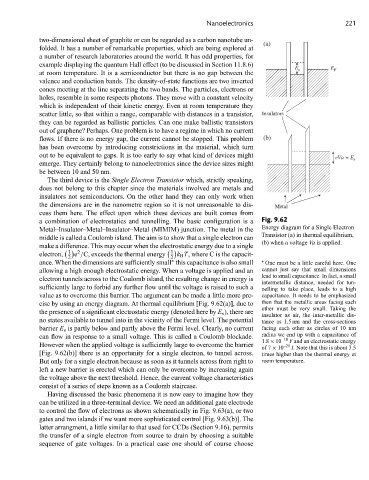
a combination of electrostatics and tunnelling. The basic configuration is a Fig. 9.62
Metal–Insulator–Metal–Insulator–Metal (MIMIM) junction. The metal in the Energy diagram for a Single Electron
Transistor (a) in thermal equilibrium,
middle is called a Coulomb island. The aim is to show that a single electron can
(b) when a voltage Va is applied.
make a difference. This may occur when the electrostatic energy due to a single
1
1
2
electron, e /C, exceeds the thermal energy k B T, where C is the capacit-
2 2
ance. When the dimensions are sufficiently small this capacitance is also small ∗ One must be a little careful here. One
∗
allowing a high enough electrostatic energy. When a voltage is applied and an cannot just say that small dimensions
lead to small capacitance. In fact, a small
electron tunnels across to the Coulomb island, the resulting change in energy is
intermetallic distance, needed for tun-
sufficiently large to forbid any further flow until the voltage is raised to such a nelling to take place, leads to a high
value as to overcome this barrier. The argument can be made a little more pre- capacitance. It needs to be emphasized
cise by using an energy diagram. At thermal equilibrium [Fig. 9.62(a)], due to then that the metallic areas facing each
other must be very small. Taking the
the presence of a significant electrostatic energy (denoted here by E s ), there are insulator as air, the inter-metallic dis-
no states available to tunnel into in the vicinity of the Fermi level. The potential tance as 1.5 nm and the cross-sections
barrier E s is partly below and partly above the Fermi level. Clearly, no current facing each other as circles of 10 nm
can flow in response to a small voltage. This is called a Coulomb blockade. radius we end up with a capacitance of
1.8 × 10 –18 F and an electrostatic energy
However when the applied voltage is sufficiently large to overcome the barrier –21
of 7 × 10 J. Note that this is about 3.5
[Fig. 9.62(b)] there is an opportunity for a single electron, to tunnel across. times higher than the thermal energy at
But only for a single electron because as soon as it tunnels across from right to room temperature.
left a new barrier is erected which can only be overcome by increasing again
the voltage above the next threshold. Hence, the current voltage characteristics
consist of a series of steps known as a Coulomb staircase.
Having discussed the basic phenomena it is now easy to imagine how they
can be utilized in a three-terminal device. We need an additional gate electrode
to control the flow of electrons as shown schematically in Fig. 9.63(a), or two
gates and two islands if we want more sophisticated control [Fig. 9.63(b)]. The
latter arrangment, a little similar to that used for CCDs (Section 9.16), permits
the transfer of a single electron from source to drain by choosing a suitable
sequence of gate voltages. In a practical case one should of course choose