
Page 238 - Electrical Properties of Materials
P. 238
220 Principles of semiconductor devices
in Fig. 9.60(a) is known as a Lateral Resonant Tunnelling Transistor. Lateral,
because the electrons move in the lateral (horizontal) direction, and resonant
because current flows only at certain resonant values of the inner gate voltage.
One can see that here is a device which can be switched by very small changes
(of the order of millivolts) in voltage. In practice, at least for the present, the
energy levels are not so well resolved, mainly due to electron scattering in the
well which will spread the electron energies. Cooling the device will help, but
we are still very far away from measuring delta functions in current. What we
do see are little current maxima at the right voltages. But these are early days.
There are a number of other devices too which have been shown to work in
the laboratory. Let me mention four of them.
Nanotube transistors. In order to make nanotube transistors we first need
nanotubes. What are they? They are thin-walled cylinders of about 1.5 nm
diameter and 25 nm long bearing strong resemblance to the fullerenes dis-
cussed in Section 5.3.6. The wall is usually made up of one single atomic
layer of carbon atoms. The process of preparing them is relatively easy. An arc
needs to be struck between graphite electrodes at the right pressure. They are
made up of graphite sheets and have their desirable properties (strong covalent
bonds) without the disadvantages (weak bonds between the layers). They are
very strong mechanically, they have both metallic and semiconductor varieties.
The problem is to get rid of the metallic variety. One of the methods to do this
is to burn them out, another is to use chemical compounds to attract metallic
and semiconductor tubes to different areas of the surface.
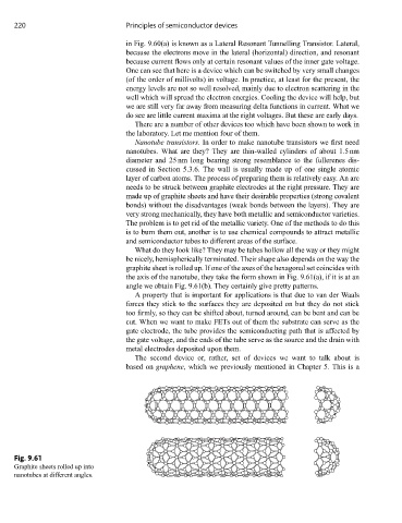
What do they look like? They may be tubes hollow all the way or they might
be nicely, hemispherically terminated. Their shape also depends on the way the
graphite sheet is rolled up. If one of the axes of the hexagonal set coincides with
the axis of the nanotube, they take the form shown in Fig. 9.61(a), if it is at an
angle we obtain Fig. 9.61(b). They certainly give pretty patterns.
A property that is important for applications is that due to van der Waals
forces they stick to the surfaces they are deposited on but they do not stick
too firmly, so they can be shifted about, turned around, can be bent and can be
cut. When we want to make FETs out of them the substrate can serve as the
gate electrode, the tube provides the semiconducting path that is affected by
the gate voltage, and the ends of the tube serve as the source and the drain with
metal electrodes deposited upon them.
The second device or, rather, set of devices we want to talk about is
based on graphene, which we previously mentioned in Chapter 5. This is a
Fig. 9.61
Graphite sheets rolled up into
nanotubes at different angles.