
Page 240 - Electrical Properties of Materials
P. 240
222 Principles of semiconductor devices
a planar configuration. The Coulomb island(s) and the two metal electrodes
would be evaporated upon one side of an insulator and the gate electrode(s)
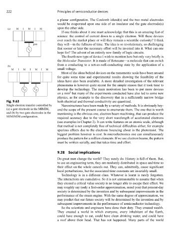
(a) M I M I M upon the other side.
If one thinks about it one must acknowledge that this is an amazing feat of
science: the control of current down to a single electron. Will these devices
ever reach the market place or will they remain a scientific curiosity? I think
gate they will—in the fullness of time. The idea is so revolutionary, so challenging
that sooner or later the necessary effort will be invested into it. What can one
V g
hope for? The advent of an entirely new family of logic circuits.
The fourth new type of device I wish to mention here but only very briefly is
the Molecular Transistor. It is made of Rotoxane—a molecule that can switch
from a conducting to a not-so-well-conducting state by the application of a
(b)
M I M I M I M small voltage.
Most of the ideas behind devices on the nanometric scale have been around
for quite some time and experimental results showing the feasibility of the
ideas have also been available. A more detailed investigation of the relevant
phenomena is however quite recent for the simple reason that it took time to
develop the technology. The main motivation has been to put more devices
V g2 V g1
2
on a mm but many of the experiments conducted have also led to some new
physics, as for example to the discovery that in a sufficiently narrow bridge
Fig. 9.63 both electrical and thermal conductivity are quantized.
Single electron transfer controlled by Nanostructures have been made by a variety of methods. It is obviously bey-
(a) a gate electrode in the MIMIM, ond the scope of the present course to enumerate them. The one that is worth
and (b) by two gate electrodes in the mentioning is the obvious one, electron beam machining, that can produce the
MIMIMIM configuration.
required accuracy due to the very short wavelength of accelerated electrons
(see examples in Chapter 2). It can write features on an atomic scale, although
that method is not completely free of technical difficulties either, for example
spurious effects due to the electrons bouncing about in the photoresist. The
biggest problem however is cost. In microelectronics one can simultaneously
produce the pattern for a million elements. If we use electron beams, the pattern
must be written serially, and that takes time and effort.
9.28 Social implications
Do great men change the world? They surely do. History is full of them. But,
to use an engineering term, they are randomly distributed in space and time so
their effect on the whole cancels out. They can, admittedly, cause significant
local perturbations, but the associated time constants are invariably small.
Technology is in a different class. Whatever is learnt is rarely forgotten.
The interactions are cumulative. So it is not unreasonable to assume that when
they exceed a critical value society is no longer able to escape their effect. We
may roughly say (only a first-order approximation, mind you) that present-day
society is determined by the invention and by subsequent improvements in the
performance of the steam engine. With the same degree of approximation, we
may predict that our future society will be determined by the invention and by
subsequent improvements in the performance of semiconductor technology.
So the scientists and engineers have done their duty. They created wealth.
They created a world in which everyone, every inhabitant of the Earth,
could have enough to eat, could have clean drinking water, and could have
a roof above their head. That has not happened. Many parts of the world