
Page 241 - Electrical Properties of Materials
P. 241
Exercises 223
are plagued by starvation and disease. Corruption is widespread. Unnecessary
wars abound.
In the developed world, there is the twin problem of unemployment in gen-
eral and over-employment in administration. People love to create work for
each other, as so ably explained by Parkinson. ∗ ∗ C. Northcote Parkinson, Parkinson’s
Any chance that the future will bring something better? We should perhaps law (John Murray, 1958).
finish this section by quoting again Gabor’s aphorism, the motto to the Intro-
duction, page xiv: ‘Till now man has been up against Nature; from now on he
will be up against his own nature’.
Exercises
9.1. Show that the ‘built-in’ voltage in a p–n junction is [Hint: Use the same argument for the conduction and diffusion
given by currents cancelling each other as in the previous example.]
kT N en kT N hp
U 0 = log e = log e , 9.4. In a metal–insulator–n-type semiconductor junction the
e N ep e N hn
dielectric constants are i and s for the insulator and the
where N en , N hn and N ep ,and N hp are the carrier densities semiconductor respectively. Taking the width of the insulator
beyond the transition region in the n and p-type materials (sufficient to prevent tunnelling) to be equal to d i ,determ-
respectively. ine the width of the depletion region as a function of reverse
[Hint: Use eqns (8.17) and (8.20) and the condition that the voltage.
Fermilevelsmustagree.]
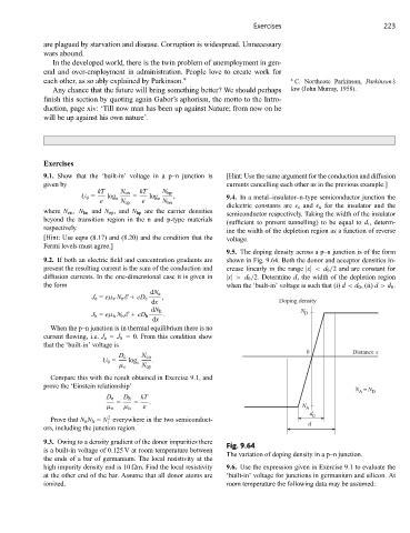
9.5. The doping density across a p–n junction is of the form
9.2. If both an electric field and concentration gradients are shown in Fig. 9.64. Both the donor and acceptor densities in-
present the resulting current is the sum of the conduction and crease linearly in the range |x| < d 0 /2 and are constant for
diffusion currents. In the one-dimensional case it is given in |x| > d 0 /2. Determine d, the width of the depletion region
the form when the ‘built-in’ voltage is such that (i) d < d 0 , (ii) d > d 0 .
dN e
J e = eμ e N e E + eD e ,
dx Doping density
dN h N
J h = eμ h N h E + eD h . D
dx
When the p–n junction is in thermal equilibrium there is no
current flowing, i.e. J e = J h = 0. From this condition show
that the ‘built-in’ voltage is
0 Distance x
D e N en
U 0 = log .
e
μ e N ep
Compare this with the result obtained in Exercise 9.1, and
prove the ‘Einstein relationship’
N = N
A D
D e D h kT
= = .
μ e μ h e N A
d 0
2
Prove that N e N h = N everywhere in the two semiconduct-
i d
ors, including the junction region.
9.3. Owing to a density gradient of the donor impurities there
Fig. 9.64
is a built-in voltage of 0.125 V at room temperature between
The variation of doping density in a p–n junction.
the ends of a bar of germanium. The local resistivity at the
high impurity density end is 10 m. Find the local resistivity 9.6. Use the expression given in Exercise 9.1 to evaluate the
at the other end of the bar. Assume that all donor atoms are ‘built-in’ voltage for junctions in germanium and silicon. At
ionized. room temperature the following data may be assumed: