
Page 236 - Electrical Properties of Materials
P. 236
218 Principles of semiconductor devices
Silicon substrate
Electrode Spacer
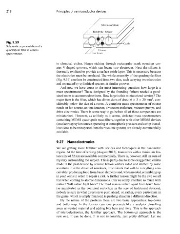
Fig. 9.59
Oxide
Schematic representation of a
quadrupole filter in a mass Groove
spectrometer. Ion beam
to chemical etches. Hence etching through rectangular mask openings cre-
ates V-shaped grooves, which can locate two electrodes. Next the silicon is
thermally oxidized to provide a surface oxide layer. This is necessary because
the electrodes must be insulated. The whole assembly of the quadrupole filter
(Fig. 9.59) can then be constructed from two dies, each carrying two electrodes
and separated by cylindrical spacers in similar grooves.
And now we have come to the most interesting question: how large is a
mass spectrometer? Those designed by the founding fathers needed a good-
sized room to accommodate them. How large is this miniaturized version? The
3
major item is the filter, which has dimensions of about 6 × 3 × 30 mm , con-
siderably below the size of a room. A complete mass spectrometer of course
needs an ion source, an ion detector, a vacuum enclosure, vacuum pumps, and
drive electronics. There is some way to go before all of these components are
miniaturized. However, as unlikely as it seems, desk-top mass spectrometers
containing MEMS quadrupole mass filters, together with other MEMS devices
(an electrospray ion source operating at atmospheric pressure and a chip that al-
lows ions to be transported into the vacuum system) are already commercially
available.
9.27 Nanoelectronics
We are getting more familiar with devices and techniques in the nanometre
region. At the time of writing (August 2013), transistors with a minimum fea-
ture size of 32 nm are available commercially. There is, however, still an aura of
mystery surrounding the subject. This is partly due to some exaggerated claims
made in the past decade by science fiction writers aided and abetted by some
scientists. It is the dream of nanobots, little robots that will do everything con-
ceivable: producing food from basic elements and, when needed, scrambling up
in your veins in order to repair a clot. A further reason might be the awe we all
feel when coming to atomic dimensions. Can we really interfere so much with
nature? Will nature fight back? The third reason is that, apart from brute force
(as manifested in the continual reduction in the size of traditional devices),
nobody is sure in what direction to push ahead; or, rather, every participant in
the game, which is amply financed, is pushing ahead in a different direction.
By the nature of the problem there are two basic approaches: top-down
and bottom-up. In the former case one proceeds like a sculptor chiselling
away unwanted material and adding bits here and there. This is the approach
of microelectronics, the familiar approach. The bottom-up approach is the
new one. It can be done. It is not impossible, just pretty difficult. Let me