
Page 233 - Electrical Properties of Materials
P. 233
Microelectro-mechanical systems (MEMS) 215
9.26 Microelectro-mechanical systems (MEMS)
Up to now, everything has been immobile. Well, nearly. Electrons had a licence
to roam about and the lattice was allowed to vibrate. The difference is that, from
now on, part of a structure can mechanically move to perform some useful
function. This is a big subject to which we are unable to do justice in the few
pages available, but we shall try to convey the essence of the idea by going in
some detail through one example (a movable mirror) and discussing the role
of a quadrupole filter in the context of a mass spectrometer.
9.26.1 A movable mirror
In the present section we shall talk about the construction of the mirror
(many of the steps in the process are similar to those discussed in relation to
microelectronic circuits). The optical aspects will be discussed in Chapter 13.
I shall start with a silicon wafer with a SiO 2 insulator on the top. We could
deposit polysilicon on the insulator, as outlined in the previous section, but
if we need a thicker layer and higher quality then another technique, called
Bonded Silicon-on-Insulator, is used. It involves the bonding of another sil-
icon wafer to the oxidized silicon substrate. The initial bonding is carried out
under ultra-clean conditions, and the assembly is then heated in a furnace to
strengthen the bond by inter-diffusion. The bonded layer may then be ground
and polished, to leave a high-quality single crystal Si layer which can be of
virtually any desired thickness.
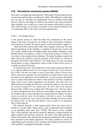
To fabricate the mirror, the bonded layer is first metal-coated, typically with
Cr to improve adhesion and then Au to improve reflectivity. This is shown in
Fig. 9.58(a). We have five layers on top of each other: silicon, silicon oxide,
silicon, chromium, and gold. The next problem is to shape both the mirror and
its elastic torsion suspension in the bonded layer. As you may guess, the bonded
layer is coated with photoresist which is then patterned with the mechanical
shape of the mirror, elastic suspension, and surround. After that come two
different kinds of etching, the first one to transfer the pattern to the metal and
the second to transfer it to the silicon layer. We arrive then at the situation
shown in Fig. 9.58(b) (cross-section) and 9.58(c) (top view). The next step is
to remove the photoresist after which the whole thing is turned upside down,
the substrate side is coated with photoresist and patterned to define a clearance
cavity (we need the cavity for the mirror to be able to move). Two further
etchings are needed now, one to remove the silicon and the next one to remove
the silicon oxide. At this point the mirror is free to rotate on its suspension
[Fig. 9.58(d) and (e)].
The released structure is then turned upside down once more and at-
tached to a second wafer, which carries a pair of patterned metal electrodes
on an insulating oxide layer [Fig. 9.58(f)]. The mirror is now complete
[Fig. 9.58(g) and (h)], and may be rotated by applying a voltage between the
upper electrode and one lower electrode. The mirror will rotate until the at-
tractive electrostatic force between the electrodes is balanced by the restoring
force provided by the elastic suspension. The elastic qualities of silicon are
surprisingly good, and there are few problems with fatigue and brittle fracture
if the assembly is packaged and handled carefully.