
Page 228 - Electrical Properties of Materials
P. 228
210 Principles of semiconductor devices
Metal
p + p + SiO
2
n
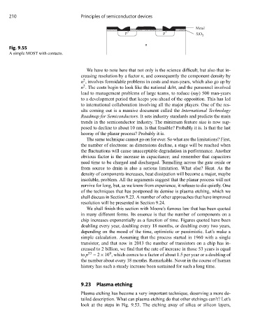
Fig. 9.55
A simple MOST with contacts.
We have to note here that not only is the science difficult, but also that in-
creasing resolution by a factor n, and consequently the component density by
2
n , involves formidable problems in costs and man-years, which also go up by
2
n . The costs begin to look like the national debt, and the personnel involved
lead to management problems of large teams, to reduce (say) 500 man-years
to a development period that keeps you ahead of the opposition. This has led
to international collaboration involving all the major players. One of the res-
ults coming out is a massive document called the International Technology
Roadmap for Semiconductors. It sets industry standards and predicts the main
trends in the semiconductor industry. The minimum feature size is now sup-
posed to decline to about 10 nm. Is that feasible? Probably it is. Is that the last
hooray of the planar process? Probably it is.
The same technique cannot go on for ever. So what are the limitations? First,
the number of electrons: as dimensions decline, a stage will be reached when
the fluctuations will cause unacceptable degradation in performance. Another
obvious factor is the increase in capacitance; and remember that capacitors
need time to be charged and discharged. Tunnelling across the gate oxide or
from source to drain is also a serious limitation. What else? Heat. As the
density of components increases, heat dissipation will become a major, maybe
insoluble, problem. All the arguments suggest that the planar process will not
survive for long, but, as we know from experience, it refuses to die quietly. One
of the techniques that has postponed its demise is plasma etching, which we
shall discuss in Section 9.23. A number of other approaches that have improved
resolution will be presented in Section 9.24.
We shall finish this section with Moore’s famous law that has been quoted
in many different forms. Its essence is that the number of components on a
chip increases exponentially as a function of time. Figures quoted have been
doubling every year, doubling every 18 months, or doubling every two years,
depending on the mood of the time, optimistic or pessimistic. Let’s make a
simple calculation. Assuming that the process started in 1960 with a single
transistor, and that now in 2013 the number of transistors on a chip has in-
creased to 2 billion, we find that the rate of increase in those 53 years is equal
9
to p 53 =2×10 , which comes to a factor of about 1.5 per year or a doubling of
the number about every 18 months. Remarkable. Never in the course of human
history has such a steady increase been sustained for such a long time.
9.23 Plasma etching
Plasma etching has become a very important technique, deserving a more de-
tailed description. What can plasma etching do that other etchings can’t? Let’s
look at the steps in Fig. 9.53. The etching away of silica or silicon layers,