
Page 222 - Electrical Properties of Materials
P. 222
204 Principles of semiconductor devices
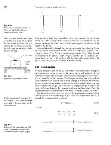
I
I
A
Fig. 9.50
The current as a function of time in
GaAs when high-field domains
t t t t t
move across the material. 0 1 2 3
Note that the transit time mode Thus, the Gunn diode has an oscillation frequency governed by the domain
is not the only mode of operation transit time. The velocity of the domain is more or less determined by the
for this GaAs oscillator. By pre- voltage producing the effect; so in practice the frequency is selected by the
venting the formation of domains length of the device.
the bulk negative resistance can be A typical Gunn diode is made by growing an epitaxial layer of n-type GaAs,
+
21
directly utilized. with an electron concentration of 10 –10 22 m –3 on to an n -substrate (con-
–3
24
centration about 10 m ). The current flow in the device (Fig. 9.51) is through
Gold wire the thickness of the epitaxial layer. For good quality GaAs the domain velo-
–1
5
city is about 10 ms ;a10 μm layer will therefore make an oscillator in the
10
n-type 10 Hz frequency band (the so-called X-band of radar).
active
n + layer
9.19 Strain gauges
Heat We have noticed before (in the case of thermal expansion) that a change in
sink
lattice dimension causes a change in the energy gap as well as in the value of
Fig. 9.51 k at the band edge. These changes will also occur if the expansion or contrac-
Sketch of a typical Gunn diode. tion is caused by applied stresses. The changes are slight and with intrinsic
semiconductors would cause only a small change in resistance. If, however,
we have a p-type semiconductor with impurities only partially ionized, a very
small change in the energy bands can cause a large percentage change in the
energy difference between the impurity levels and the band edge. Thus, the
change in resistance of the material with stress (or strain) is large (Fig. 9.52).
Semiconductor strain gauges are pieces of semiconductor with two ohmic
contacts that are of a suitable shape to glue on to the component under test. In
K is a geometrical constant, L is general, the resistance R can be written
the length, A the cross-sectional
area, and ρ the resistivity of the R = K(ρL/A). (9.29)
semiconductor.
Thus,
dR dL dA dρ
= – + , (9.30)
R L A ρ
Impurity level Shift due to lattice strain
Fig. 9.52
The shift of the energy diagram with
strain; this makes semiconductors Shift due to lattice strain
suitable materials for strain gauges. Valence band