
Page 204 - Electrical Properties of Materials
P. 204
186 Principles of semiconductor devices
If we could get energy like this out of a simple circuit isolated from the rest
of the world except for the R, L, and C we have drawn, it would contravene the
second law of thermodynamics and make perpetual motion fairly straightfor-
ward. As this does not happen, we can conclude that a ‘negative resistance’ has
to be an active circuit device that is connected to a power supply other than the
oscillating signal with which it interacts. This is very true of the tunnel diode,
since to act as a negative resistance, it has to be biased with a battery to the
point A in Fig. 9.25(c). The power to overcome the circuit losses comes from
this battery.
If the magnitude of the negative resistance in Fig. 9.25(c) is greater than
the loss resistance R, the initiatory signal will not only persist; it will grow. Its
magnitude will, of course, be limited by the fact that the tunnel diode can be a
negative resistance for only a finite voltage swing (about 0.2 V). Thus, given a
negative resistance circuit engineers can make oscillators and amplifiers. The
particular advantage of tunnel diodes is that, as the junctions are thin, the car-
rier transit times are shorter than in a transistor, and high-frequency operation
11
(up to about 10 Hz) is possible. Their limitation is that with their inherently
low voltage operation, they are very low-power devices.
I
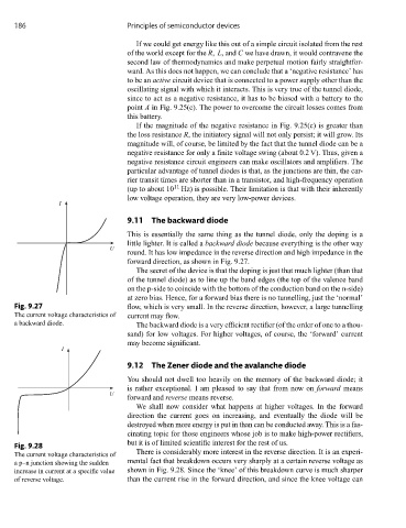
9.11 The backward diode
This is essentially the same thing as the tunnel diode, only the doping is a
little lighter. It is called a backward diode because everything is the other way
U
round. It has low impedance in the reverse direction and high impedance in the
forward direction, as shown in Fig. 9.27.
The secret of the device is that the doping is just that much lighter (than that
of the tunnel diode) as to line up the band edges (the top of the valence band
on the p-side to coincide with the bottom of the conduction band on the n-side)
at zero bias. Hence, for a forward bias there is no tunnelling, just the ‘normal’
Fig. 9.27 flow, which is very small. In the reverse direction, however, a large tunnelling
The current voltage characteristics of current may flow.
a backward diode. The backward diode is a very efficient rectifier (of the order of one to a thou-
sand) for low voltages. For higher voltages, of course, the ‘forward’ current
may become significant.
I
9.12 The Zener diode and the avalanche diode
You should not dwell too heavily on the memory of the backward diode; it
is rather exceptional. I am pleased to say that from now on forward means
U
forward and reverse means reverse.
We shall now consider what happens at higher voltages. In the forward
direction the current goes on increasing, and eventually the diode will be
destroyed when more energy is put in than can be conducted away. This is a fas-
cinating topic for those engineers whose job is to make high-power rectifiers,
but it is of limited scientific interest for the rest of us.
Fig. 9.28
There is considerably more interest in the reverse direction. It is an experi-
The current voltage characteristics of
a p–n junction showing the sudden mental fact that breakdown occurs very sharply at a certain reverse voltage as
increase in current at a specific value shown in Fig. 9.28. Since the ‘knee’ of this breakdown curve is much sharper
of reverse voltage. than the current rise in the forward direction, and since the knee voltage can