Page 199 - Electrical Properties of Materials
P. 199

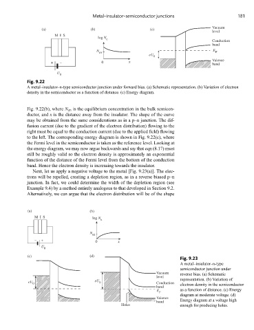
Metal–insulator–semiconductor junctions                      181

                                                                                           Vacuum
                    ) a (                ) b (                    ) c (
                                                                                           level
                        M  I  S
                                          log N
                                              e
                                                                                           Conduction
                                                                                           band
                                          N                                                E
                                           en                                               F
                                                                eU
                                                                  0
                       +  –                 0          x                                   Valence
                                                                                           band
                          U
                          0
            Fig. 9.22
            A metal–insulator–n-type semiconductor junction under forward bias. (a) Schematic representation. (b) Variation of electron
            density in the semiconductor as a function of distance. (c) Energy diagram.

            Fig. 9.22(b), where N en is the equilibrium concentration in the bulk semicon-
            ductor, and x is the distance away from the insulator. The shape of the curve
            may be obtained from the same considerations as in a p–n junction. The dif-
            fusion current (due to the gradient of the electron distribution) flowing to the
            right must be equal to the conduction current (due to the applied field) flowing
            to the left. The corresponding energy diagram is shown in Fig. 9.22(c), where
            the Fermi level in the semiconductor is taken as the reference level. Looking at
            the energy diagram, we may now argue backwards and say that eqn (8.17) must
            still be roughly valid so the electron density is approximately an exponential
            function of the distance of the Fermi level from the bottom of the conduction
            band. Hence the electron density is increasing towards the insulator.
               Next, let us apply a negative voltage to the metal [Fig. 9.23(a)]. The elec-
            trons will be repelled, creating a depletion region, as in a reverse biased p–n
            junction. In fact, we could determine the width of the depletion region (see
            Example 9.4) by a method entirely analogous to that developed in Section 9.2.
            Alternatively, we can argue that the electron distribution will be of the shape


             (a)                       (b)
                M  I  S                 log N
                                           e

                                       N
                                        en
                –  +                     0         x
                   U
                    0
             (c)                       (d)
                                                                             Fig. 9.23
                                                                             A metal–insulator–n-type
                                                                             semiconductor junction under
                                                                   Vacuum    reverse bias. (a) Schematic
                                                                   level
             eU                          eU 0                                representation. (b) Variation of
               0                                                   Conduction  electron density in the semiconductor
                                                                   band
                                                                   E         as a function of distance. (c) Energy
                                                                    F
                                                                             diagram at moderate voltage. (d)
                                                                   Valence
                                                                   band      Energy diagram at a voltage high
                                                    Holes                    enough for producing holes.
   194   195   196   197   198   199   200   201   202   203   204