
Page 195 - Electrical Properties of Materials
P. 195
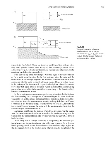
Metal–semiconductor junctions                        177

               (a)
                        φ M                        φ S     φ B  Conduction band

                                                             E FS
              E
               FM
                                                              Valence band


               (b)

                         φ M                φ –φ            Conduction band
                                φ –φ B       M  S        φ S
                                 M
              E
               FM                                          E                 Fig. 9.16
                                                            FS
                                                                             Energy diagrams for a junction
                                                                             between a metal and an n-type
                                                                             semiconductor (φ M >φ S ), (a) before
                                                                             contact, (b) after contact the Fermi
                                                            Valence band
                                                                             levels agree (E FM = E FS ).


            material, in Fig. 9.16(a). These are shown as solid lines. Now with an infin-
            itely small gap the vacuum levels are equal; thus, we may join them with a
            dotted line in Fig. 9.16(b); the conduction and valence band edge must also be
            continued parallel to the vacuum level.
               What can we say about the charges? We may argue in the same fashion
            as for a metal–metal junction. In the first instance, when the metal and the
            semiconductor are brought together, the electrons from the conduction band
            cross over into the metal in search of lower energy. Hence a certain region
            in the vicinity of the junction will be practically depleted of mobile carriers.
            So we may talk again about a depletion region and about the accompanying
            potential variation, which is incidentally, the same thing as the ‘band-bending’
            obtained from the band picture.
               So the two pictures are complementary to a certain extent. In the first one
            the ‘band-bending’ is a consequence of the matching of the Fermi levels and
            vacuum levels, and the charge imbalance follows from there. In the second pic-
            ture electrons leave the semiconductor, causing a charge imbalance and hence
            a variation in the potential energy. Whichever way we look at it, the outcome
            is a potential barrier between the metal and the semiconductor. Note that the
            barrier is higher from the metal side.
               In dynamic equilibrium the number of electrons crossing over the barrier
            from the metal to the semiconductor is equal to the number crossing over the
            barrier from the semiconductor side. We may say that the current I 0 flows in
            both directions.
               Let us apply now a voltage; according to the polarity, the electrons’ po-
            tential energy on the semiconductor side will go up or down. For a forward
            bias it goes up, which means that we have to draw the band edges higher up.
            But the vacuum level at the junction stays where it was. So the effect of the