
Page 190 - Electrical Properties of Materials
P. 190
172 Principles of semiconductor devices
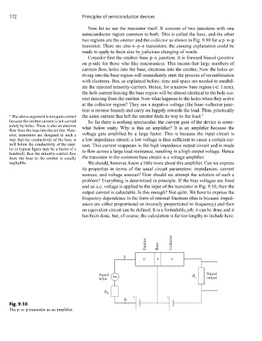
Now let us see the transistor itself. It consists of two junctions with one
semiconductor region common to both. This is called the base, and the other
two regions are the emitter and the collector as shown in Fig. 9.10 for a p–n–p
transistor. There are also n–p–n transistors; the ensuing explanation could be
made to apply to them also by judicious changing of words.
Consider first the emitter–base p–n junction. It is forward biased (positive
on p-side for those who like mnemonics). This means that large numbers of
carriers flow, holes into the base, electrons into the emitter, Now the holes ar-
riving into the base region will immediately start the process of recombination
with electrons. But, as explained before, time and space are needed to annihil-
ate the injected minority-carriers. Hence, for a narrow base region ( 1 mm),
the hole current leaving the base region will be almost identical to the hole cur-
rent entering from the emitter. Now what happens to the holes when they arrive
at the collector region? They see a negative voltage (the base–collector junc-
tion is reverse biased) and carry on happily towards the load. Thus, practically
∗ the same current that left the emitter finds its way to the load. ∗
The above argument is not quite correct
because the emitter current is not carried So far there is nothing spectacular; the current gain of the device is some-
solely by holes. There is also an electron what below unity. Why is this an amplifier? It is an amplifier because the
flow from the base into the emitter. How-
ever, transistors are designed in such a voltage gets amplified by a large factor. This is because the input circuit is
way that the conductivity of the base is a low impedance circuit; a low voltage is thus sufficient to cause a certain cur-
well below the conductivity of the emit- rent. This current reappears in the high impedance output circuit and is made
ter (a typical figure may be a factor of a
hundred); thus the minority-carrier flow to flow across a large load resistance, resulting in a high output voltage. Hence
from the base to the emitter is usually the transistor in the common base circuit is a voltage amplifier.
negligible. We should, however, know a little more about this amplifier. Can we express
its properties in terms of the usual circuit parameters: impedances, current
sources, and voltage sources? How should we attempt the solution of such a
problem? Everything is determined in principle. If the bias voltages are fixed
and an a.c. voltage is applied to the input of the transistor in Fig. 9.10, then the
output current is calculable. Is this enough? Not quite. We have to express the
frequency dependence in the form of rational fractions (this is because imped-
ances are either proportional or inversely proportional to frequency) and then
an equivalent circuit can be defined. It is a formidable job; it can be done and it
has been done, but, of course, the calculation is far too lengthy to include here.
Emitter Base Collector
A
P n P
input ~ R L Signal
Signal
output
R
S
+ +
B
Fig. 9.10
The p–n–p transistor as an amplifier.