
Page 194 - Electrical Properties of Materials
P. 194
176 Principles of semiconductor devices
but in computers. Admittedly, computers did exist before the advent of the
transistor, but they were bulky, clumsy, and slow. The computers you know
and respect, from giant ones down to pocket calculators, depend on the good
services of transistors. One could easily write a thousand pages about the cir-
I cuits used in various computers—the trouble is that by the time the thousandth
c
U E page is jotted down, the first one is out of date. The rate of technical change in
this field is simply breathtaking, much higher than ever before in any branch
R of technology. Fortunately, the principles are not difficult. For building a logic
circuit all we need is a device with two stable states, and that can be easily
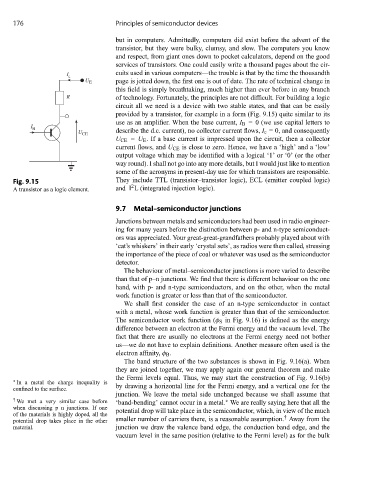
provided by a transistor, for example in a form (Fig. 9.15) quite similar to its
use as an amplifier. When the base current, I B = 0 (we use capital letters to
I
B
U CE describe the d.c. current), no collector current flows, I c = 0, and consequently
U CE = U E . If a base current is impressed upon the circuit, then a collector
current flows, and U CE is close to zero. Hence, we have a ‘high’ and a ‘low’
output voltage which may be identified with a logical ‘1’ or ‘0’ (or the other
way round). I shall not go into any more details, but I would just like to mention
some of the acronyms in present-day use for which transistors are responsible.
Fig. 9.15 They include TTL (transistor–transistor logic), ECL (emitter coupled logic)
2
A transistor as a logic element. and I L (integrated injection logic).
9.7 Metal–semiconductor junctions
Junctions between metals and semiconductors had been used in radio engineer-
ing for many years before the distinction between p- and n-type semiconduct-
ors was appreciated. Your great-great-grandfathers probably played about with
‘cat’s whiskers’ in their early ‘crystal sets’, as radios were then called, stressing
the importance of the piece of coal or whatever was used as the semiconductor
detector.
The behaviour of metal–semiconductor junctions is more varied to describe
than that of p–n junctions. We find that there is different behaviour on the one
hand, with p- and n-type semiconductors, and on the other, when the metal
work function is greater or less than that of the semiconductor.
We shall first consider the case of an n-type semiconductor in contact
with a metal, whose work function is greater than that of the semiconductor.
The semiconductor work function (φ S in Fig. 9.16) is defined as the energy
difference between an electron at the Fermi energy and the vacuum level. The
fact that there are usually no electrons at the Fermi energy need not bother
us—we do not have to explain definitions. Another measure often used is the
electron affinity, φ B .
The band structure of the two substances is shown in Fig. 9.16(a). When
they are joined together, we may apply again our general theorem and make
the Fermi levels equal. Thus, we may start the construction of Fig. 9.16(b)
∗ In a metal the charge inequality is
confined to the surface. by drawing a horizontal line for the Fermi energy, and a vertical one for the
junction. We leave the metal side unchanged because we shall assume that
† We met a very similar case before ‘band-bending’ cannot occur in a metal. We are really saying here that all the
∗
when discussing p–n junctions. If one potential drop will take place in the semiconductor, which, in view of the much
of the materials is highly doped, all the †
potential drop takes place in the other smaller number of carriers there, is a reasonable assumption. Away from the
material. junction we draw the valence band edge, the conduction band edge, and the
vacuum level in the same position (relative to the Fermi level) as for the bulk