
Page 198 - Electrical Properties of Materials
P. 198
180 Principles of semiconductor devices
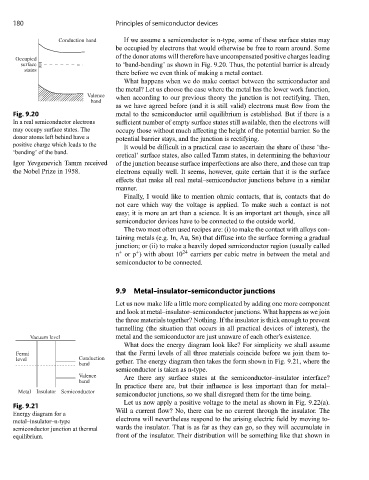
Conduction band If we assume a semiconductor is n-type, some of these surface states may
be occupied by electrons that would otherwise be free to roam around. Some
of the donor atoms will therefore have uncompensated positive charges leading
Occupied
surface to ‘band-bending’ as shown in Fig. 9.20. Thus, the potential barrier is already
states
there before we even think of making a metal contact.
What happens when we do make contact between the semiconductor and
the metal? Let us choose the case where the metal has the lower work function,
Valence when according to our previous theory the junction is not rectifying. Then,
band
as we have agreed before (and it is still valid) electrons must flow from the
Fig. 9.20 metal to the semiconductor until equilibrium is established. But if there is a
In a real semiconductor electrons sufficient number of empty surface states still available, then the electrons will
may occupy surface states. The occupy those without much affecting the height of the potential barrier. So the
donor atoms left behind have a potential barrier stays, and the junction is rectifying.
positive charge which leads to the It would be difficult in a practical case to ascertain the share of these ‘the-
‘bending’ of the band.
oretical’ surface states, also called Tamm states, in determining the behaviour
Igor Yevgenevich Tamm received of the junction because surface imperfections are also there, and those can trap
the Nobel Prize in 1958. electrons equally well. It seems, however, quite certain that it is the surface
effects that make all real metal–semiconductor junctions behave in a similar
manner.
Finally, I would like to mention ohmic contacts, that is, contacts that do
not care which way the voltage is applied. To make such a contact is not
easy; it is more an art than a science. It is an important art though, since all
semiconductor devices have to be connected to the outside world.
The two most often used recipes are: (i) to make the contact with alloys con-
taining metals (e.g. In, Au, Sn) that diffuse into the surface forming a gradual
junction; or (ii) to make a heavily doped semiconductor region (usually called
+
+
n or p ) with about 10 24 carriers per cubic metre in between the metal and
semiconductor to be connected.
9.9 Metal–insulator–semiconductor junctions
Let us now make life a little more complicated by adding one more component
and look at metal–insulator–semiconductor junctions. What happens as we join
the three materials together? Nothing. If the insulator is thick enough to prevent
tunnelling (the situation that occurs in all practical devices of interest), the
Vacuum level metal and the semiconductor are just unaware of each other’s existence.
What does the energy diagram look like? For simplicity we shall assume
Fermi that the Fermi levels of all three materials coincide before we join them to-
level Conduction gether. The energy diagram then takes the form shown in Fig. 9.21, where the
band
semiconductor is taken as n-type.
Valence Are there any surface states at the semiconductor–insulator interface?
band
In practice there are, but their influence is less important than for metal–
Metal Insulator Semiconductor
semiconductor junctions, so we shall disregard them for the time being.
Let us now apply a positive voltage to the metal as shown in Fig. 9.22(a).
Fig. 9.21
Will a current flow? No, there can be no current through the insulator. The
Energy diagram for a
electrons will nevertheless respond to the arising electric field by moving to-
metal–insulator–n-type
semiconductor junction at thermal wards the insulator. That is as far as they can go, so they will accumulate in
equilibrium. front of the insulator. Their distribution will be something like that shown in