
Page 326 - Electrical Properties of Materials
P. 326
308 Lasers
3. They have high efficiency.
4. They operate at low voltage.
5. They are small.
6. They are robust.
7. They have long life.
8. The technique for their production is suitable for mass manufacture, so
they are potentially inexpensive.
9. They can be produced in arrays.
10. They may be made to work in the wavelength range in which optical fibres
have favourable loss (near to minimum) and dispersion properties.
I am sure if I tried hard, I could come up with a few more advantages but, I
think, ten are enough to show that semiconductor lasers merit special attention.
How does a semiconductor laser work? The basic idea is very simple. It is
radiative recombination in a direct-gap semiconductor which leads eventually
to laser action. Why a direct gap? Because we want the probability of a trans-
ition from the bottom of the conduction band to the top of the valence band
to be high. What else do we need? We need a piece of material in which there
are lots of electrons in the conduction band eager to descend, and in which
there are lots of empty states at the top of the valence band eager to receive the
electrons. A homogeneous piece of semiconductor is obviously not suitable
because we cannot achieve both conditions simultaneously, only one at a time.
But that gives an idea. We can have lots of electrons in a degenerate (discussed
in Section 9.10 when talking of tunnel diodes) n-type semiconductor and, sim-
ilarly, we can have lots of holes in a degenerate p-type semiconductor. So let
us put them together, that is, produce a p–n junction, and then in the middle of
it both conditions may be expected to be satisfied, provided the forward bias,
U 1 , is close to the energy gap.
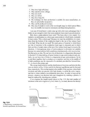
The energy band structure and the distribution of electrons and holes for this
case are shown in Fig. 12.8(a) and (b) for thermal equilibrium and for forward
bias, respectively. The overlap region in the middle of the junction, where both
electrons and holes are present with high density, is called the active region,
and that is where radiative recombination takes place. In order to keep up the
process, whenever an electron–hole pair disappears by emitting a photon, it
must be replaced by injecting new carriers.
If we examine the simple model shown in Fig. 12.9, the total number of
electrons in the active region is N e lwd, where N e , as usual, denotes the density
) a ( ) b (
eU ≈E
Photon 1 g
emission
E
F
Fig. 12.8
A degenerate p–n junction at (a) p n
thermal equilibrium, (b) forward bias.