
Page 327 - Electrical Properties of Materials
P. 327
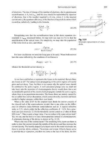
Semiconductor lasers                        309

            of electrons. The rate of change of the number of electrons, due to spontaneous
            recombination, is N e lwd/t rec , and this loss should be replenished by injection  Active
            of electrons, that is the number required is (I i /e)η, where I i is the injected  I  region
            current and η, the quantum efficiency, is the fraction of injected electrons which
            recombine radiatively, leading to the formula
                                                                                                       d
                                      N e lwd  I i η
                                            =   .                    (12.35)
                                        t rec  e
                                                                                                w
               Recognizing now that the recombination time in the above equation cor-  l
            responds to t spont discussed before, we may now use eqn (12.31) to find the
                                                                             Fig. 12.9
            amplification of the optical wave. For simplicity, we may take the population
                                                                             Schematic representation of a laser
            of the lower level as zero, and obtain
                                                                             diode.
                                           2
                                          c g(ν)η
                                  γ (ν)=           I i .             (12.36)
                                            2 2
                                         8πn ν elwd
               For laser oscillations we need the loop gain to be unity. When both mirrors
            have the same reflectivity, the condition of oscillation is

                                    R exp(γ – α)l = 1,               (12.37)

            whence the threshold current density is
                                       2 2
                               I i  8πn ν ed     1
                                  =           α – 1n R .             (12.38)
                                     2
                               lw    c ηg(ν)     l
               As we have said before α represents the losses in the material. But are there
            any losses at all? The optical wave propagating in the active region will surely
            grow and not decay. True, but there is no reason why the optical wave should
            be confined to the active region. A well calculated plunge (one we shall not
            take here) into the mysteries of electromagnetic theory would show that a not
            inconsiderable portion of the electric field propagates outside the active region,
            where there is no population inversion. The losses there are mainly caused by
            the so-called free-carrier absorption, which comes about by electrons and holes
            excited to higher energies within their own bands.
               What is the value of R? In the simplest laser diode the mirror consists of
            the cleaved end of the semiconductor crystal, that is one relies on the differ-
            ence in refractive index between semiconductor and air. A typical refractive
            index is 3.35, which yields for the reflection coefficient, R = 0.54. For a prac-
            tical case (see Exercise 12.10) the threshold current comes to a value of about
                    –2
            820 A cm . This is quite a large value. Can we reduce it by some clever trick?
            Yes, we can, and the trick is to use a heterojunction instead of a homojunction.
            A schematic drawing of the device is shown in Fig. 12.10.
               What is the role of the various layers? The insulating SiO 2 layers are there in
            order to steer the current towards the middle of the device and thus increase the
            current density. The heavily doped GaAs layers next to the metal electrodes are
            there to provide ohmic contacts. The p-type and n-type AlGaAs layers serve
            to provide the p–n junction, and then we come to the star of the show, the thin