
Page 335 - Electrical Properties of Materials
P. 335
Semiconductor lasers 317
The nitrides have added another facet to bandgap engineering. Generally
among the III–Vs we find that large lattice spacing corresponds to small energy
gap—see the extremes of InSb and GaP in Fig. 12.15; nitrogen is the smallest
atom we consider in the semiconductor components of Table 8.2, even smal-
ler than carbon and boron which have lower atomic numbers and weights. So
adding N as an isoelectronic replacement for As or P will decrease the mean
lattice spacing, but the highly electronegative and piezoelectric nature of N
∗
means that the bandgap is reduced by the large bowing factor. There is an ∗ When Ga and In are mixed in the
interesting group called the ‘Gina’ alloys (Ga In N As). Gallium arsenide has proportion of 1 – x and x, one would
expect the resulting energy gap to be
the most advanced technology of all the III–Vs so it is much in demand as
E g (Ga 1–x In x N) = (1 – x)E g (GaN) +
a substrate, good quality slices are available to grow on other compounds by xE g (InN), but the actual energy gap turns
MBE or MOCVD. However they have to be lattice matched. From Fig. 12.15 out to be smaller. An empirical formula
it can be seen that GaAlAs will lattice match all the way to AlAs, that is the gives the reduction in the form bx(1 – x)
bandgap can go to 2.2 eV well into the visible. Now by adding N and In to where b is called the bowing factor. In
any case it is difficult to predict the exact
GaAs it is possible to keep the mean lattice spacing constant (N goes down, In energy gap owing to the fact that ni-
up), provided the added concentrations of In and N are in the ratio of 3:1. Both trides do not form large single crystals or
these materials reduce the energy gap. So a Gina alloy to lattice match GaAs uniform alloys. There are compositional
variations and strains as well as piezo-
is Ga 1–3x In 3x N x As 1–x . An example is 3x = 0.53 which gives a bandgap of
electric effects throughout the MOCVD
0.74 eV. These infrared alloys have been used to make lasers to match the de- layers.
sirable optical fibre wavelength of 1.3 μm, and for solar cells. At the other end
of the spectrum, the shortest wavelength of 342 nm (corresponding to a gap of
3.6 eV) was achieved with a GaN compound which contained no indium.
What should we do if we wish to have a high power semiconductor laser?
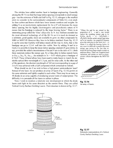
Instead of one laser, we can produce an array of lasers (Fig. 12.16) grown on
the same substrate and lightly coupled to each other. There may be as many as
40 diodes in an array capable of producing several watts of output power. The
difficulty is to persuade all the lasers to radiate in phase.
Next, I wish to mention a relatively new development in which the diode
Fig. 12.16
lasers emit light in the same direction as the current flows. They are called An array of lasers.
Vertical Cavity Surface Emitting Lasers. Their structure is shown in Fig. 12.17.
Top contact
Bragg
reflectors
Active
layer
Bragg
reflectors
Fig. 12.17
Substrate
Light output Schematic representation of a Vertical
Cavity Surface Emitting Laser.