
Page 333 - Electrical Properties of Materials
P. 333
Semiconductor lasers 315
First, how to make them. We know how to produce quantum wells. The
obvious way of making quantum dots is then to etch away the other two di-
mensions. This was indeed tried, and the dots produced worked in a fashion
but not very well. The reason was the high density of surface states created
during etching. The technique used nowadays is strained-layer epitaxy. It is
called self-organized because the quantum dots organize themselves. How?
Let us talk about growing InAs on GaAs. The mismatch between their lat-
tices is about 7%, causing strain. After the growth of a few monolayers the
∗
strain becomes unbearable, and the layers break up and create 3D islands. ∗ In more sophisticated language, one
Once the growth of the islands starts, it quickly reaches saturation. Typical should say that after a critical thickness,
8
–2
quantum dot densities may vary between 10 and 10 11 cm . The shapes are the increasing strain between the layers
makes it energetically favourable for the
quasi-pyramidal with a base of 10–20 nm and a height of 3–10 nm. In order strain to be relieved by formation of 3D
to incorporate these dots into a device they need to be ‘capped’, i.e. filled up islands.
with a material, which would be GaAs in the present case. During the capping
process, as may be expected, the heights of the InAs islands collapse down to
maybe 2 nm after a GaAs cap of 2 nm.
An obvious way of increasing the number of quantum dots is to have more
layers. With the materials mentioned above, another layer of InGaAs needs to
be deposited, and then one can repeat the same procedure. An atomic force mi-
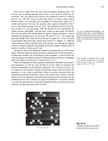
†
croscopy image of a bilayer structure (in this case the second layer of quantum † The number of quantum dots in Fig.
dots is just above the first layer) is shown in Fig. 12.14. 12.14 can be counted to be 31. Since this
2
When will quantum dot lasers appear commercially? Reliable mass produc- is for an area of 0.25 μm , the density
–2
comes to 1.24 × 10 10 cm .
tion techniques are still far away, but that is not all. There are actually still
unresolved problems concerning their operation. The emission process is not
as simple as it first appears, because the relevant energy levels are nearly de-
generate, i.e. very close to each other. When an electron descends from the
conduction band and recombines with a hole it does emit a photon, but that
photon may be immediately reabsorbed by promoting another electron into the
conduction band. This is known as Auger recombination. A possible remedy
is to coat the quantum dot with another material which can localize electrons
and holes on opposing sides of the interface.
Fig. 12.14
A highly uniform dot ensemble
0.5 m × 0.5 m produced by self-organization.