
Page 336 - Electrical Properties of Materials
P. 336
318 Lasers
The active layer still consists of multiple quantum wells. The main difference
is that the Bragg reflectors are at the top and bottom. They can be produced
by the same techniques as the wells, and they can be made highly reflective. In
λ λ 0,0 the realization of Fig. 12.17, the reflector at the top has a reflection coefficient
λ 0,1 λ 1,0
0,2 λ very near to unity, whereas the reflection coefficient of the bottom reflector
2,0
is somewhat smaller, allowing the radiation to come through the transparent
substrate. The area of the laser can now be made very small leading to even
smaller threshold currents ( 0.1 mA). A further advantage is the ease with
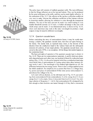
which arrays can be made. A two-dimensional array is shown in Fig. 12.18,
where each microlaser may work at the same wavelength (to produce a high
output) or may be tuned to different wavelengths.
12.7.4 Quantum cascade lasers
Fig. 12.18
An array of VCSEL lasers. Before concluding the story of semiconductor lasers, it may be worth men-
tioning a relative, the quantum cascade laser, that does not quite belong to
the family. The family trait, as repeated many times, is the descent of the
electron from the conduction band to the valence band and the subsequent
emission of a photon, of one single photon. The quantum cascade laser, con-
ceived in the early 1970s, is an exception. All the things that matter happen in
the conduction band.
The basic principle of operation of the quantum cascade laser is shown in
Fig. 12.19. There are two semiconductor materials, A and B, which are altern-
ately deposited upon each other (say, one hundred of them) by molecular beam
epitaxy (Fig. 12.19). A is the active material which has a conduction band edge
much below that of semiconductor B. Lasing action takes place between en-
ergy levels 1 and 2. The wavelength of the emitted light depends on E,the
difference between the two energy levels. There is also a voltage applied across
the whole sandwich. For simplicity let us assume that there is a voltage drop,
V B across each piece of semiconductor B but none across semiconductor A,
and choose this voltage to be eV B .
Let’s start with an electron, on the left-hand end of Fig. 12.19, just enter-
ing from semiconductor B into semiconductor A at the energy level 2. It sees
energy level 1 to be empty. Hence it descends from level 2 to level 1 by emit-
ting a photon of frequency f = E/h. But semiconductor B is designed to be
thin enough so that electrons can tunnel through it if they find a convenient
B
A
B
A
Level 2
B
A
B
ΔE
Level 1
Fig. 12.19
Energy diagram for a quantum
cascade laser.