
Page 372 - Electrical Properties of Materials
P. 372
354 Optoelectronics
counterparts. It looks as though optical communications can come about on
a wide scale, without the benefit of integrated optics, so unless there is some
new and urgent impetus provided by the need to develop optical computers or
some other forms of optical processing, further progress is likely to remain
slow. Nevertheless, it is a very promising technique, so I must give at least an
introduction to its basic precepts.
13.7.1 Waveguides
The principle is very simple. If a material exhibiting a certain index of refrac-
tion is surrounded by a material of lower index of refraction, then a wave may
be guided in the former material by successive total internal reflections. Optical
fibres (mentioned before) represent one such possibility for guiding waves, but
that is not suitable for integrated optics. We can however rely on the fact that
the refractive index of GaAs is higher than that of AlGaAs and, consequently, a
GaAs layer grown on the top of AlGaAs will serve as a waveguide. As may be
seen in Table 13.2, GaAs is an electro-optic crystal, it is also suitable for pro-
ducing junction lasers, microwave oscillators, and transistors. Thus, altogether,
GaAs seems to be the ideal material for integrated optics. Well, it is indeed the
ideal material, but the problems of integration have not as yet been solved. It
is still very much at the laboratory stage.
Nearer to commercial application are the LiNbO 3 devices, which I shall
describe in more detail. In these devices the waveguides are produced by indif-
fusing Ti into a LiNbO 3 substrate through appropriately patterned masks (the
same kind of photolithography we met in Section 9.22 when discussing integ-
rated circuits). Where Ti is indiffused the refractive index increases sufficiently
to form a waveguide.
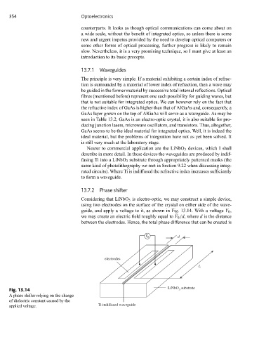
13.7.2 Phase shifter
Considering that LiNbO 3 is electro-optic, we may construct a simple device,
using two electrodes on the surface of the crystal on either side of the wave-
guide, and apply a voltage to it, as shown in Fig. 13.14. With a voltage V 0 ,
we may create an electric field roughly equal to V 0 /d, where d is the distance
between the electrodes. Hence, the total phase difference that can be created is
V 0 d
electrodes
L
LiNbO substrate
Fig. 13.14 3
A phase shifter relying on the change
of dielectric constant caused by the
applied voltage. Ti indiffused waveguide