
Page 385 - Electrical Properties of Materials
P. 385
Electro-absorption in quantum well structures 367
effect is the description used for the shift and splitting of energy levels in an
electric field. It earned the 1919 Nobel Prize
Talking of electro-absorption, I should also mention the Franz–Keldysh ef- for Stark. He was the only Nobel
fect, which is usually observed at electric fields considerably higher than that prizewinner who became a strong
needed to see the effect upon exciton resonance. It bears some similarity to the supporter of Nazism. His job (he
Schottky effect (see Section 6.6), in which electrons excited thermally to high did it very well) was to ‘purify’
enough energy levels could tunnel across a barrier made thin by the presence of German universities of ‘contamin-
a high electric field. For the Franz–Keldysh effect, the energy is provided by an ated blood’. The ‘impure’ refugees
input photon with an energy less than the bandgap energy, and then tunnelling from German and Austrian univer-
can do the rest to provide an electron–hole pair. sities played a large part in defeat-
ing Nazism.
13.11.4 Applications
If I had to classify the quantum confined Stark effect in literary terms, I would
not quite know where to place it. Perhaps melodrama would be the right cat-
egory, considering the touching affection between electrons and holes. If we
consider, however, how they stave off brutal intervention by the electric field,
with their backs against the potential wall, and how quickly all these things
happen, then melodrama might give way to a thriller. And that is certainly the
category to which our ultimate question belongs: ‘can these effects be used for
something?’
Well, if the attenuation of the device depends on the electric field, then the
amount of light across it may be modulated by changing the applied voltage.
We need relatively high fields, which we know may be achieved by placing
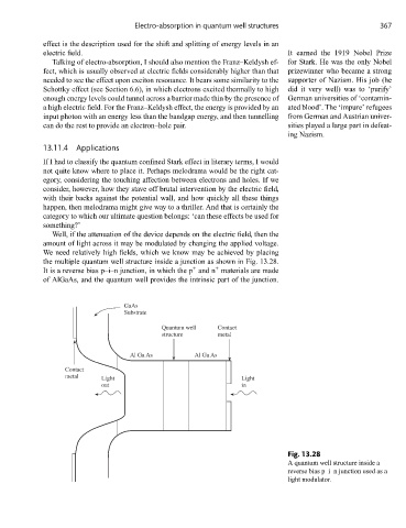
the multiple quantum well structure inside a junction as shown in Fig. 13.28.
+
+
It is a reverse bias p–i–n junction, in which the p and n materials are made
of AlGaAs, and the quantum well provides the intrinsic part of the junction.
GaAs
Substrate
Quantum well Contact
structure metal
Al Ga As Al Ga As
Contact
metal Light Light
out in
Fig. 13.28
A quantum well structure inside a
reverse bias p–i–n junction used as a
light modulator.