
Page 387 - Electrical Properties of Materials
P. 387
Exercises 369
Let us now summarize the advantages of multiple quantum well structures
for the applications discussed. The main advantage is compatibility, that is the
voltages are compatible with the electronics, and the wavelengths are compat-
ible with laser diodes. In addition, the materials are compatible with those used
both in electronics and for laser diodes, so the devices are potential candidates
for components in integrated opto-electronic systems.
I have only mentioned GaAs–AlGaAs structures, but there are, of course,
others as well. The rules are clearly the same, that apply to the production of
heterojunction lasers. The lattice constants must be close, and the bandgaps
must be in the right range. Interestingly, some of the combinations offer quite
new physics; for example in an InAs–GaSb quantum well, the electrons are
confined in one layer and the holes in the other.
As you may have gathered, I find this topic quite fascinating, so perhaps I
have spent a little more time on it than its present status would warrant. I hope
youwill forgiveme.
Exercises
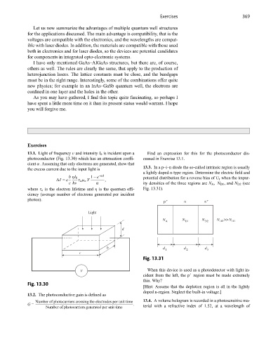
13.1. Light of frequency ν and intensity I 0 is incident upon a Find an expression for this for the photoconductor dis-
photoconductor (Fig. 13.30) which has an attenuation coeffi- cussed in Exercise 13.1.
cient α. Assuming that only electrons are generated, show that
13.3. In a p–i–n diode the so-called intrinsic region is usually
the excess current due to the input light is
a lightly doped n-type region. Determine the electric field and
b ηI 0 1– e –αd potential distribution for a reverse bias of U r when the impur-
I = e τ e μ e V ,
c hν α ity densities of the three regions are N A , N D1 ,and N D2 (see
where τ e is the electron lifetime and η is the quantum effi- Fig. 13.31).
ciency (average number of electrons generated per incident
photon). + +
p n n
Light
N N N N N
A D1 D2 D2 D1
d
b d d d
1 2 3
c
Fig. 13.31
V When this device is used as a photodetector with light in-
+
cident from the left, the p region must be made extremely
thin. Why?
Fig. 13.30
[Hint: Assume that the depletion region is all in the lightly
doped n-region. Neglect the built-in voltage.]
13.2. The photoconductive gain is defined as
Number of photocarriers crossing the electrodes per unit time 13.4. A volume hologram is recorded in a photosensitive ma-
G = .
Number of photocarriers generated per unit time terial with a refractive index of 1.52, at a wavelength of