
Page 386 - Electrical Properties of Materials
P. 386
368 Optoelectronics
P in
R
–
P
i Quantum well
V 0
n
+
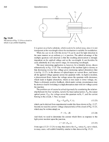
Fig. 13.29
The device of Fig. 13.24 in a circuit in
P out
which it can exhibit bistability.
It is grown on a GaAs substrate, which needs to be etched away, since it is not
transparent at the wavelength where the mechanism is suitable for modulation.
What else can we do with this device? It can be used for light detection in
the same manner as an ordinary p–i–n junction. The added advantage of the
multiple quantum well structure is that the resulting photocurrent is strongly
dependent on the applied voltage and on the wavelength. It can therefore be
used, admittedly in a very narrow range, for measuring wavelength.
The most interesting application is, however, for a bistable device, shown
schematically in Fig. 13.29. The wavelength of the incident light is chosen, so
that decreasing reverse bias voltage gives increasing optical absorption (line
A in Fig. 13.27). In the absence of optical input, no current flows, and hence
all the applied voltage appears across the quantum wells. As light is incident,
a photocurrent flows, hence the voltage across the quantum wells decreases,
which leads to higher absorption, which in turn leads to lower voltage, etc.
There is obviously positive feedback, which under certain circumstances may
be shown to lead to switching to a high absorption state with low voltage across
the junction.
The problem can of course be solved rigorously by considering the relation-
ship between the four variables, namely the input optical power, P in , the output
optical power, P out , the voltage across the quantum wells, V, and the current
flowing in the circuit, I. First, we need
P out = P out (P in , V, λ), (13.23)
which can be derived from experimental results like those shown in Fig. 13.27.
Second, we need the current–voltage characteristics of the circuit of Fig. 13.25,
which may be written simply as
V = V 0 – IR. (13.24)
And third, we need to determine the current which flows in response to the
light power incident upon the junction,
I = I(V, P in , λ). (13.25)
From eqns (13.23–13.25) we may then derive the P out versus P in curve which,
in many cases, will exhibit bistability similar to that shown in Fig. 13.23.