
Page 382 - Electrical Properties of Materials
P. 382
364 Optoelectronics
without any cross-talk. And, besides, a single mirror can switch an enormous
amount of information from fibre A to fibre B, and may be a 100 Gigabits or
may be even more in the future. Who would worry then about a switching time
that might be a few milliseconds?
13.11 Electro-absorption in quantum well structures
This is a fairly new phenomenon with potential for device applications. We
shall include it not only because it might become a winner (it is rather hazard-
ous to predict which device will prove to be commercially competitive), but
also because it is such a good illustration of a number of physical principles
discussed in this course. We shall touch upon such topics as the confinement
of electrons and holes to a certain region by the erection of potential barriers,
the modification of semiconductor absorption characteristics when excitons
(bound electron–hole pairs) are taken into account, what happens to excitons
in a potential well, how an electric field influences the energy levels, and in par-
ticular, how it affects confined excitons (known as the Quantum Confined Stark
Effect), and finally, how these varied phenomena can be exploited in devices.
I have already talked a lot about quantum wells. One of the examples we
looked at was made of GaAs and AlGaAs. For our present purpose, it is import-
ant that the wells are wide enough for tunnelling to be negligible, but narrow
enough so that the electrons and holes know that they are not in an infinitely
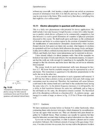
Absorption thick material.
The energy levels in such two-dimensional wells were discussed in Sec-
tion 12.7. We know that the available energies may be represented by a set of
sub-bands. The momentum is quantized in the direction perpendicular to the
walls, but not in the other two.
Let us consider now optical absorption in such a quantum well material. It
is still true that when a photon excites an electron–hole pair, both energy and
0 100 200 momentum must be conserved. Therefore, the transitions will occur between
hf - E (meV)
g a sub-band in the valence band and a sub-band in the conduction band, having
the same value of n. As the photon frequency increases, it is still possible, for
Fig. 13.25
a while, to find transitions between the same two sub-bands, and as long as
Absorption as a function of excess
the sub-bands are the same, the absorption remains constant. The theoretical
photon energy for bulk material
plot of the absorption coefficient as a function of hf – E g (photon energy – gap
(continuous lines) and 30 nm-thick
energy) is a series of steps, as shown in Fig. 13.25 for a 30 nm-wide quantum
quantum well material (dotted lines).
well.
13.11.1 Excitons
We have mentioned excitons before in Section 9.4, rather facetiously, when
contrasting them with electron–hole pairs, which disappear by recombination.
Let me say again what excitons are. They are electron–hole pairs bound to-
gether by Coulomb forces. Their existence can usually be ignored, but they
must be taken into account when looking at optical absorption on a fine scale.
Up to now we have argued that, in order to absorb a photon and to create
an electron–hole pair, the minimum amount of energy is the gap energy. How-
ever, if we take excitons into account, then we may realize that photons incident