
Page 119 - Embedded Microprocessor Systems Real World Design
P. 119
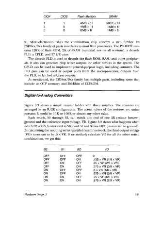
ClOF       ClOS      Flash Memory        SRAM
                            1            1         4MB x 16        500K x 16
                            1           0          4MB x 16         1MBx8
                            0           0          8MB x 8          1MBx8


                ST  Microelectronics  takes  the  combination  chip  concept  a  step  further.  Its
                PSD8xx/Sxx family of parts interfaces to most &bit processors. The PSD813F con-
                tains 128K of flash ROM, 2K of SRAM  (optional, not on all versions), a decode
                PLD, a CPLD, and 27 I/O  pins.
                   The decode PLD is used to decode the flash ROM, RAM, and other peripher-
                als. It also can generate chip select outputs for other devices in the system. The
                CPLD can be used to implement general-purpose logic, including counters. The
                1/0 pins  can  be  used  as output  ports  from  the  microprocessor, outputs  from
                the PLD, or latched address outputs.
                   As mentioned, the PSDSxx/Sxx  family has multiple parts, including some that
                include an OTP memory, and 256Kbits of EEPROM.


                Digital-to-Analog Converters


                Figure  3.3 shows a  simple resistor ladder with  three  switches. The resistors are
                arranged in  an R/2R  configuration. The actual values of  the resistors are unim-
                portant; R could be 10K or lOOK or almost any other value.
                   Each  switch, SO  through  S2, can  switch one  end of  one  2R  resistor between
                ground and the reference input voltage, VR. Figure 3.3 shows what happens when
                switch S2 is ON (connected to VR) and S1 and SO  are OFF (connected to ground).
                By calculating the resulting series/parallel resistor network, the final output voltage
                 (VO) turns out to be .5 x VR. If we similarly calculate VO for all the other switch
                combinations, we get this:


                            s2         s1        so               vo

                            OFF       OFF        OFF       0
                            OFF       OFF        ON        ,125 x VR (1/8 x VR)
                            OFF       ON         OFF       .25 x VR (2/8 x VR)
                            OFF       ON         ON        .375 x VR (3/8 x VR)
                            ON        OFF        OFF       .5 x VR (4/8 x VR)
                            ON        OFF        ON        .625 x VR (518 x VR)
                            ON        ON         OFF       .75 x VR  (6/8 x VR)
                            ON        ON         ON        .875 x VR  (7/8 x VR)


                Hardware Design 2                                                    101