
Page 115 - Embedded Microprocessor Systems Real World Design
P. 115
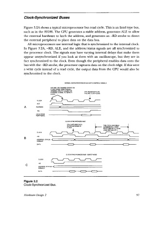
Clock-Synchronized Buses


                Figure 3.2A shows a typical microprocessor bus read cycle. This is an Intel type bus,
                such as in the 80186. The CPU generates a stable address, generates ALE to allow
                the external hardware to latch the address, and generates an -RD  strobe to direct
                the external peripheral to place data on the data bus.
                  All microprocessors use internal logic that is synchronized to the internal clock.
                In Figure 3.2A, -RD, ALE,  and the address/status signals are all synchronized to
                the processor clock. The signals may have varying internal delays that make them
                appear unsynchronized if  you look at them with an oscilloscope, but they are in
                fact synchronized to the clock. Even though the peripheral enables data onto the
                bus with the -RD  strobe, the processor captures data on the clock edge. If this were
                a write cycle instead of  a read cycle, the output data from the CPU would also be
                synchronized to the clock.


                                         NORMAL MICROPROCESSOR BUS WITH COMROL SIGNALS
                                ME AW -RD CWE STATES ON
                                CLDCKEDQE. EXENTHOUGH
                                IHTEWL DELAYS CAUSE THE
                                EXTERNAL SIGNAL TO SWITCH   CFU READS DATA ON
                                                      FALLING CLOCK EDGE
                                LATER.
                                                         I
                        CLOCK
                        ALE
                A      ADDRESS
                        -RD
                        DATA FROM
                        PERIWERAL
                                          CLOCK-SYNCHRONIZED  Bus
                                           CFU CAPTURES DATA   I   THS CYCLE WS BEEN   I
                                           ON RISING €DOE OF
                                           CLOCK
                                              4                  LOm) INSTW OF 2
                        CLOCK
                                7
                        -AS
                B       ADDRESS. STATUS  <     X             X                  X
                        SIGNAM
                        DATA

                                          CLOCKSYNCHRONIZED BUS - BURST MODE
                         CLOCK
                                 7
                         -AS
                 C       ADDRESS. STATUS <   /
                         SIWS
                         DATA

                Figure 3.2
                Clock-Synchronized Bus.


                Hardware Design 2                                                     97