
Page 335 - Embedded Microprocessor Systems Real World Design
P. 335
Connecting outputs in this way is not considered a valid design practice. When this condi-
tion occurs it is called output contention or bus contention. The term output Contention usually
refers to a single signal, and bus contention refers to a group of signals, such as a micre
processor data bus.
Some digital devices can sink current in the low state but do not source current in the
high state. These usually are the same as their current-sourcing siblings but without the
transistor in the output stage that sources current. If the logic is a bipolar family, such as
TTL, these outputs are referred to as open-collector. If the logic family is CMOS, these outputs
are called opendruin. Open-collector/-drain outputs are designed to be tied together. If one
output goes low while the other is high, no damage will occur since the high output does
not source current. Open-collector/drain signals normally are pulled high with a resistor
so that the signal will be in a valid high state when none of the outputs is driving it low.
Basic Logic Functions
Simple Gates
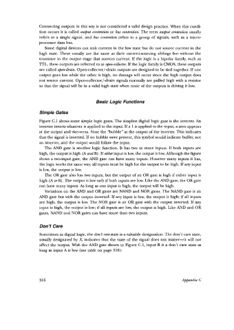
Figure C.1 shows some simple logic gates. The simplest digital logic gate is the inverter. An
inverter inverts whatever is applied to the input. If a 1 is applied to the input, a zero appears
at the output and vice-versa. Note the “bubble” at the output of the inverter. This indicates
that the signal is inverted. If no bubble were present, this symbol would indicate buffer, not
an inverter, and the output would follow the input.
The AND gate is another logic function. It has two or more inputs. If both inputs are
high, the output is high (A andB). If eitherinput is low, the output is low. Although the figure
shows a tweinput gate, the AND gate can have many inputs. However many inputs it has,
the logic works the same way; all inputs must be high for the output to be high. If any input
is low, the output is low.
The OR gate also has two inputs, but the output of an OR gate is high if either input is
high (A mB). The output is low only if both inputs are low. Like the AND gate, the OR gate
can have many inputs. As long as one input is high, the output will be high.
Variations on the AND and OR gates are NAND and NOR gates. The NAND gate is an
AND gate but with the output inverted. If any input is low, the output is high; if all inputs
are high, the output is low. The NOR gate is an OR gate with the output inverted. If any
input is high, the output is low; if all inputs are low, the output is high. Like AND and OR
gates, NAND and NOR gates can have more than two inputs.
Don’t Care
Sometimes in digital logic, the don’t cure state is a valuable designation. The don’t care state,
usually designated by X indicates that the state of the signal does not matter-it will not
affect the output. With the AND gate shown in Figure C.1, input B is a don’t care state as
long as input A is low (see table on page 318):
316 Appendix C