
Page 346 - Embedded Microprocessor Systems Real World Design
P. 346
REGISTER BANK Y
Y3
YZ
“ Y1
L
YO
f
Y-REGISTER ONTR L INPUTS
REGISTER BANK 2
23
ALU OUTPUT -
22
“
z1
L
zo
Y 8 2 REGISTER SELECT +-
ALU CONTROL INPUTS
+-’
CLOCK TO ONE REGISTER 1-
IN BANK Y OR 2. CLOCKS
RESULT INTO REGISTER
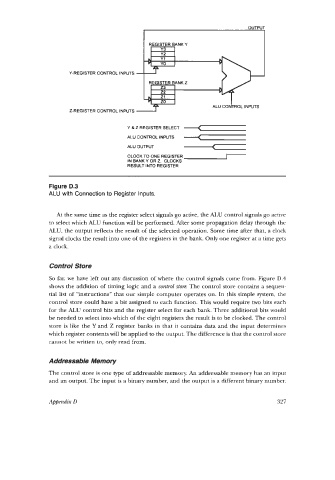
Figure D.3
ALU with Connection to Register Inputs.
At the same time as the register select signals go active, the ALU control signals go active
to select which ALU function will be performed. After some propagation delay through the
ALU, the output reflects the result of the selected operation. Some time after that, a clock
signal clocks the result into one of the registers in the bank. Only one register at a time gets
a clock.
Control Store
So far, we have left out any discussion of where the control signals come from. Figure D.4
shows the addition of timing logic and a control store. The control store contains a sequen-
tial list of “instructions” that our simple computer operates on. In this simple system, the
control store could have a bit assigned to each function. This would require two bits each
for the ALU control bits and the register select for each bank. Three additional bits would
be needed to select into which of the eight registers the result is to be clocked. The control
store is like the Y and Z register banks in that it contains data and the input determines
which register contents will be applied to the output. The difference is that the control store
cannot be written to, only read from.
Addressable Memory
The control store is one type of addressable memory. An addressable memory has an input
and an output. The input is a binary number, and the output is a different binary number.
Appendix D 327