
Page 345 - Embedded Microprocessor Systems Real World Design
P. 345
CONTROLINPUTS! A ' B
A B OUTWT
0 0 Y+Z
0 1 NOTY NEGATION
1 0 YhZ LOGICAL'AND'
1 1 Y#Z LOGICAL'OR
Figure D.l
Simple ALU.
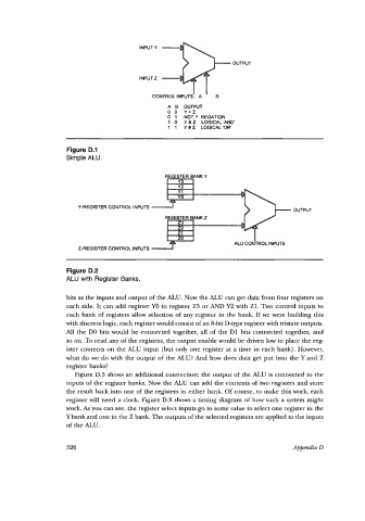
REGISTER BANK Y
Y3
Y2
Y1
YO
Y-REGISTER CONTROL INPUTS
OUTPUT
REGISTER BANK Z
23
22
21
20
f ALU CONTROL INPUTS
2-REGISTER CONTROL INPUTS
Figure D.2
ALU with Register Banks.
bits as the inputs and output of the ALU. Now the ALU can get data from four registers on
each side. It can add register YO to register 23 or AND Y2 with Z1. Two control inputs to
each bank of registers allow selection of any register in the bank. If we were building this
with discrete logic, each register would consist of an 8-bit D-type register with tristate outputs.
All the DO bits would be connected together, all of the D1 bits connected together, and
so on. To read any of the registers, the output enable would be driven low to place the reg-
ister contents on the ALU input (but only one register at a time in each bank). However,
what do we do with the output of the ALU? And how does data get put into the Y and Z
register banks?
Figure D.3 shows an additional connection; the output of the ALU is connected to the
inputs of the register banks. Now the ALU can add the contents of two registers and store
the result back into one of the registers in either bank. Of course, to make this work, each
register will need a clock. Figure D.3 shows a timing diagram of how such a system might
work. As you can see, the register select inputs go to some value to select one register in the
Y bank and one in the Z bank. The outputs of the selected registers are applied to the inputs
of the ALU.
326 Appendix D