
Page 91 - Embedded Microprocessor Systems Real World Design
P. 91
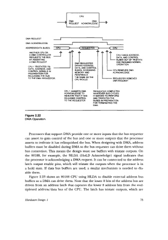
DMA REQUEST
                 DMA ACKNOWLEDGE
                ADDRESSIDATA BUSES   cw    )-----(REQUESTER   >-<    C W
                   A DMA CONTROLLER  f.
                   ANOTHER CPU OR
                   REQUESTS THE BUS                                    CPU TAKES ADDRESS.
                                                                       DATA, AND CONTROL
                   BY ASSERTING                                        BUSES OUT OF TRISTATE
                   A DMA REQUEST                                       AND RESUMES NORMAL
                                                                       OPERATION
                  CPU 1 TRISTATES ITS
                  DATA, ADDRESS, AND          BUSES, ACCESSING  LL CPU REMOVES DMA
                  CONTROL SIGNALS IN
                  PREPARATION FOR                                    ACKNOWLEDGE
                  RELEASING THE BUS
                  TO THE DMA REQUESTOR.       THE SAME AS THE   - REQUESTER REMOVES
                                              CW WOULD.              DMA REQUEST
                                        CW  1 ASSERTS DMA   REQUESTER COMPLETES
                                        ACKNOWLEDGE TO   WHATEVER BUS CYCLES
                                        INDICATE THAT IT HAS   IT NEEDED TO PERFORM
                                        RELEASED CONTROL   AND TRISTATES THE
                                        TO THE REQUESTER   BUSES IN PREPARATION
                                                         FOR TERMINATING THE
                                                         DMA.

                Figure 2.22
                DMA Operation.


                  Processors that support DMA provide one or more inputs that the bus requester
                can assert to gain control of  the bus and one or more outputs that the processor
                asserts to indicate it has relinquished the bus. When designing with DMA, address
                buffers must be disabled during DMA so the bus requester can drive them without
                bus contention. This means the design must use buffers with tristate outputs. On
                the  80188, for  example, the  HLDA  (HOLD Acknowledge) signal indicates that
                the processor is acknowledging a DMA request. It can be connected to the address
                latch output enable pins, which will  tristate the outputs when the processor is in
                a hold  state. If data bus buffers are used, a similar mechanism is needed to dis-
                able them.
                  Figure 2.23 shows an 80188 CPU using HLDA to disable external address bus
                buffers so a DMA can drive them. Note that the lower 8 bits of the address bus are
                driven from an address latch that captures the lower 8 address bits from the mul-
                tiplexed address/data bus of  the CPU. The latch has tristate outputs, which are


                Hardware Design I                                                     75