
Page 87 - Embedded Microprocessor Systems Real World Design
P. 87
I'C TIMING
SCL -1
START
SDA
DATABIT SCL
CLOCKINO
SDA - % X -
MICROWIRE TIMING
SI(
DIIDO --X->
-cs 7
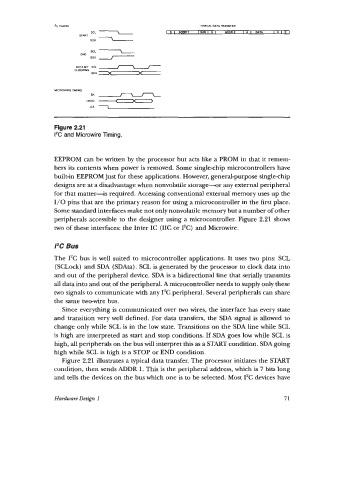
Figure 2.21
1% and Microwire Timing.
EEPROM can be written by the processor but acts like a PROM in that it remem-
bers its contents when power is removed. Some singlechip microcontrollers have
built-in EEPROM just for these applications. However, general-purpose singlechip
designs are at a disadvantage when nonvolatile storage-or any external peripheral
for that matter-is required. Accessing conventional external memory uses up the
1/0 pins that are the primary reason for using a microcontroller in the first place.
Some standard interfaces make not only nonvolatile memory but a number of other
peripherals accessible to the designer using a microcontroller. Figure 2.21 shows
two of these interfaces: the Inter IC (IIC or 1%) and Microwire.
1% Bus
The 1% bus is well suited to microcontroller applications. It uses two pins: SCL
(SCLock) and SDA (SDAta). SCL is generated by the processor to clock data into
and out of the peripheral device. SDA is a bidirectional line that serially transmits
all data into and out of the peripheral. A microcontroller needs to supply only these
two signals to communicate with any 1% peripheral. Several peripherals can share
the same twewire bus.
Since everything is communicated over two wires, the interface has every state
and transition very well defined. For data transfers, the SDA signal is allowed to
change only while SCL is in the low state. Transitions on the SDA line while SCL
is high are interpreted as start and stop conditions. If SDA goes low while SCL is
high, all peripherals on the bus will interpret this as a START condition. SDA going
high while SCL is high is a STOP or END condition.
Figure 2.21 illustrates a typical data transfer. The processor initiates the START
condition, then sends ADDR 1. This is the peripheral address, which is 7 bits long
and tells the devices on the bus which one is to be selected. Most 12C devices have
Hardware Design 1 71